NT3980 データシートの表示(PDF) - Novatek Microelectronics
部品番号
コンポーネント説明
メーカー
NT3980 Datasheet PDF : 13 Pages
| |||
NT3980
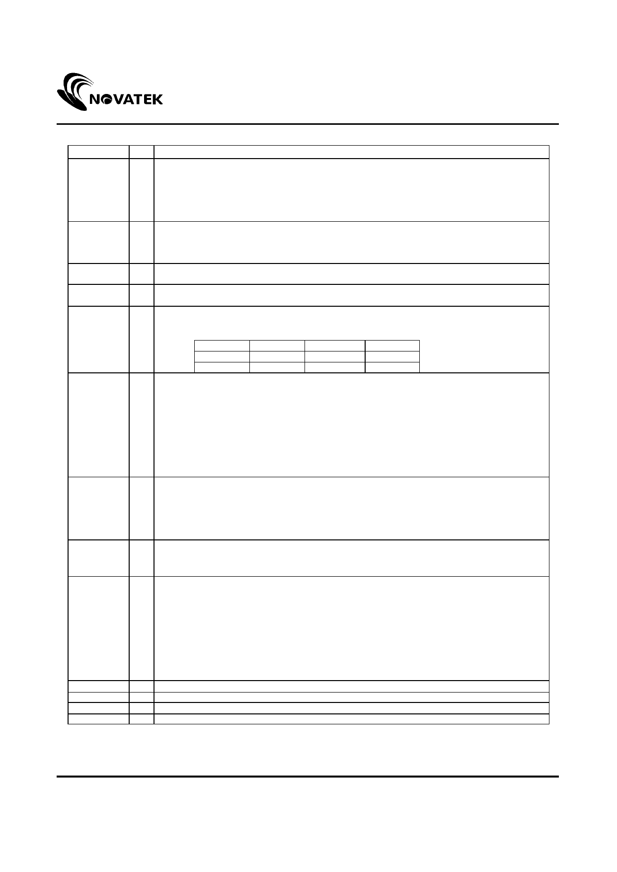
TFT LCD Source Driver
Pin Description
Designation
D07 ~ D00
D17 ~ D10
D27 ~ D20
D37 ~ D30
D47 ~ D40
D57 ~ D50
REV1
REV2
V1 ~ V10
OUT1 ~
OUT384
SHL
DIO1
DIO2
LD
CLK
I/O
Description
Data input. For six 8-bit data,2 pixels, of color data (R, G, B)
I DX7 : MSB; DX0 : LSB
I Controls whether data are inverted or not.
When “REVx”=1 the data will be inverted. EX. “00” à “ FF”, “07”à “ F8”, “15”à “EA”, and so on.
REV1: control D0x to D2x ,REV2: control D3x to D5x .
(These two pins can be connected together on TCP.)
I Gamma correction reference voltage. The voltage of these pins must be AVSS< V10< V9<
V8<V7<V6; V5<V4<V3<V2<V1< AVDD
O Output drive signals;
I Selects left or right shift;
SHL=“1” : DIO1 →OUT1,2,3,4,5,6→OUT7,8,9,10,11,12--→OUT379,380,381,382,383,384= DIO2
SHL=“0” : DIO1=OUT1,2,3,4,5,6←OUT7,8,9,10,11,12←-- OUT379,380,381,382,383,384←DIO2
SHL
DIO1
DIO2
SHIFT
1
Input
Output
Right
0
Output
Input
Left
I/O Start pulse signal input/output
When SHL is applied high (SHL=”1”), a start high-pulse on DIO1 is latched at the rising edge of the
CLK. Then the data are latched serially onto internal latches at the rising edge of the CLK. After all
line latches are filled with data, 64 clocks , a pulse is shifted out through the DIO2 pin at the rising
edge of the CLK. This function can cascade two or more devices for dot expansion. In normal
applications, the DIO2 signal of the first device is connected to the DIO1 of the second stage, the
DIO2 of the second one is connected to the DIO1 of the third, and so on, like a daisy chain.
In contrast, when SHL is applied low, a start pulse inputs on DIO2, and a pulse outputs through
DIO1.
*Remark : The input pulse-width of DIO1/2 may exceed 1 clock-cycle.
I Latches the polarity of outputs and switches the new data to outputs.
1.At the rising edge, the pin latches the “POL” signal to control the polarity of the outputs.
2.This pin also controls the switch of the line registers that switches the new incoming data
to outputs.
*Remark: The LD may switch the new data to outputs at anytime even if the line data are not
completely full.
I Clock input; latching data onto the line latches at the rising edge .
After a start pulse input, display data latching is halted automatically after 64 clock cycles.
*Remark: At least one CLK cycle is necessary during the high -level period of LD.
POL
AVDD
AVSS
Vcc
GND
I Polarity selector for the dot-inversion control. Available at the rising edge of LD.
“POL” value is latched at the rising edge of “LD” to control the polarity of the even or odd outputs.
“POL=1” indicates that even outputs are of positive polarity with a voltage range from V1~V5, and
odd outputs are of negative polarity with a voltage range from V6 to V10. On the other hand, if LD
receives low level “POL”, even outputs are of negative polarity and odd outputs are of positive
polarity.
POL=1: Even outputs range from V1 ~ V5
Odd outputs range from V6 ~ V10
POL=0: Even outputs range from V6 ~ V10
Odd outputs range from V1 ~ V5
I Power supply for analog circuit;
I Ground pin for analog circuit
I Power supply for digital circuit
I Ground pin for digital circuit
Version 1.0
3
October 16, 2001
Share Link: 