ASCELL3911 データシートの表示(PDF) - austriamicrosystems AG
部品番号
コンポーネント説明
メーカー
ASCELL3911 Datasheet PDF : 13 Pages
| |||
ISM 868 MHz, 433 MHz and 315 MHz FSK Transmitter – Preliminary Data Sheet
ASCell3911
Austria Mikro Systeme International AG
The ASCell3911 WAKEUP pin is active and set to ”L”, holding the µC in reset state. In standby
mode the ASCell3911 WAKEUP internal pull-up is disabled and does not drain current from the
supply.
The ASCell3911 µC_CLK output is disabled, (in high resistive ”Z” state) and internally pulled up
to ”H”.
(Re)starting the transmitter: Closing the push button (giving a falling edge on µC_CLK line)
starts up the ASCell3911. It turns on its XTAL oscillator and after the oscillator start up phase it
turns the µC_CLK pin to active (CMOS level) mode and provides a clock to the µC.
After a delay of 32 µC clock cycles the WAKEUP pin of the ASCell3911 is set to ”H” for 16 clock
cycles. The transmitter is now in active mode. The WAKEUP acts in ASCell3911 active mode
as an input waiting for a ”L” to trigger the transmission of the transmitter to standby mode
During this active mode the µC sends the 132 bit data (8 bit control and 16 * 8 bit data) on the
µC - P1 (Serial data out) line.
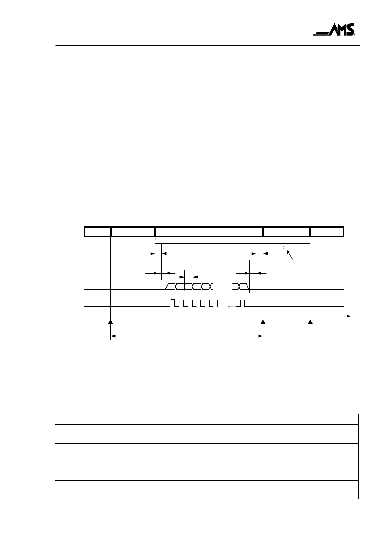
The timing of the microcontroller interface is shown in Figure 5. The microcontroller clocks a
134-bit Data into the ASCell3911 for data encoding. This data consists of 6 control bits followed
by 128 transmit data bits. After the data bock has been completely transferred to the AS-
Cell3911, it starts up transmission, during which the I/Q modulator and power amplifier are pow-
ered up in order to transmit the encoded data. Transmission is done with respect to the control
bits. Table 2 shows the control bits set different operation modes of the chip.
TX-State standby startup/reset µC
P4
D_EN
DATA
Twe
Te d
D_CLK
active
Tde
Tbit
transmission
standby
Tet
SMT
wake up
t
Twt
start
stop
transmission transmission
Figure 5:
µC interface timing for data transmission when ASCell3911 and µC are active.
Note: Figure 4 shows the timing for the CMT-mode where the controller sets P4 to “L” and so the transmission stops. The
broken line shows the Signal P4 in the SMT mode where the ASCell3911 stops the transmission.
Control bit description:
bit# Name
1
Quartz crystal (“CRYSTAL”):
2
Operating frequency range (“RANGE”):
3
Duty cycle operation (“DCO”)
4
Single / Continuous Message Transmission
(“SMT/CMT”)
Comments
L=13,5600 / 13,5672MHz
H=19,6875 MHz
L=315/433MHz,
H=868,3MHz
L = OFF
H = ON
L = SMT
H = CMT
Rev. A, February 2000
Page 7 of 13
Share Link: 