JAN7905K(2001) データシートの表示(PDF) - Microsemi Corporation
部品番号
コンポーネント説明
メーカー
JAN7905K Datasheet PDF : 7 Pages
| |||
SG7900A/SG7900 SERIES
NEGATIVE REGULATOR
CONNECTION DIAGRAMS & ORDERING INFORMATION (See Notes Below)
Package
Part No.
Ambient
Temperature Range
Connection Diagram
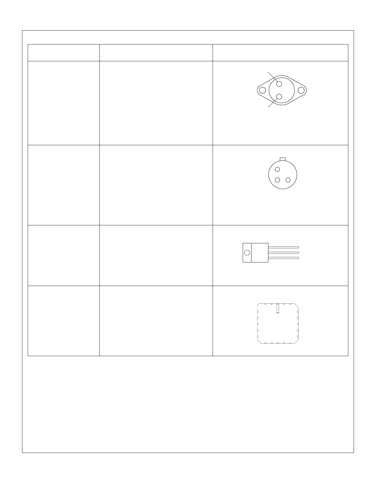
3-TERMINAL TO-3
METAL CAN
K-PACKAGE
SG79XXAK/883B
SG7905AK/DESC
SG7912AK/DESC
SG7915AK/DESC
SG79XXAK
SG79XXK/883B
JAN7905K
JAN7912K
JAN7915K
SG79XXK
SG79XXK
-55°C to 125°C
-55°C to 125°C
-55°C to 125°C
-55°C to 125°C
-55°C to 125°C
-55°C to 125°C
-55°C to 125°C
-55°C to 125°C
-55°C to 125°C
-55°C to 125°C
0°C to 125°C
GROUND
1
2
VOUT
CASE IS V
IN
3-PIN TO-39 METAL CAN
T-PACKAGE
SG79XXAT/883B
SG7905AT/DESC
SG7912AT/DESC
SG7915AT/DESC
SG79XXAT
SG79XXT/883B
JAN7905T
JAN7912T
JAN7915T
SG79XXT
-55°C to 125°C
-55°C to 125°C
-55°C to 125°C
-55°C to 125°C
-55°C to 125°C
-55°C to 125°C
-55°C to 125°C
-55°C to 125°C
-55°C to 125°C
-55°C to 125°C
GROUND 1
V
2
OUT
3
VIN
CASE IS V
IN
3-PIN HERMETIC TO-257
IG-PACKAGE (Isolated)
SG79XXAIG/883B
SG7905AIG/DESC
SG7912AIG/DESC
SG7915AIG/DESC
SG79XXAIG
SG79XXIG/883B
SG79XXIG
-55°C to 125°C
-55°C to 125°C
-55°C to 125°C
-55°C to 125°C
-55°C to 125°C
-55°C to 125°C
-55°C to 125°C
20-PIN CERAMIC
LEADLESS CHIP CARRIER
L- PACKAGE
SG79XXL/883B
SG79XXL
SG7905AL/DESC
SG7912AL/DESC
SG7915AL/DESC
-55°C to 125°C
-55°C to 125°C
-55°C to 125°C
-55°C to 125°C
-55°C to 125°C
VOUT
V
IN
GROUND
(See Notes 5 & 6)
1. N.C.
2. VIN
3. N.C.
4
4. VO
5. VO
5
6. N.C.
6
7. VO SENSE 7
8. N.C.
9. N.C.
8
10. N.C.
3 2 1 20 19
11. N.C.
12. N.C.
13. N.C.
18
14. N.C.
17 15. GND
16 16. N.C.
15
17. GND
18. N.C.
14
19. N.C.
9 10 11 12 13
20. VIN
Note 1. Contact factory for JAN and DESC product availability.
2. All parts are viewed from the top.
3. "XX" to be replaced by output voltage of specific fixed regulator.
4. Some products will be available in hermetic flat pack (F). Consult factory for price and availability.
5. Both inputs and outputs must be externally connected together at the device terminals.
6. For normal operation, the VO SENSE pin must be externally connected to the load.
05/01 Rev 1.5
Copyright 1999
LINFINITY Microelectronics Inc.
11861 Western Avenue ∞ Garden Grove, CA 92841
7
(714) 898-8121 ∞FAX: (714) 893-2570
Share Link: 