NJU3430 データシートの表示(PDF) - Japan Radio Corporation
部品番号
コンポーネント説明
メーカー
NJU3430
Japan Radio Corporation

NJU3430 Datasheet PDF : 18 Pages
| |||
NJU3430
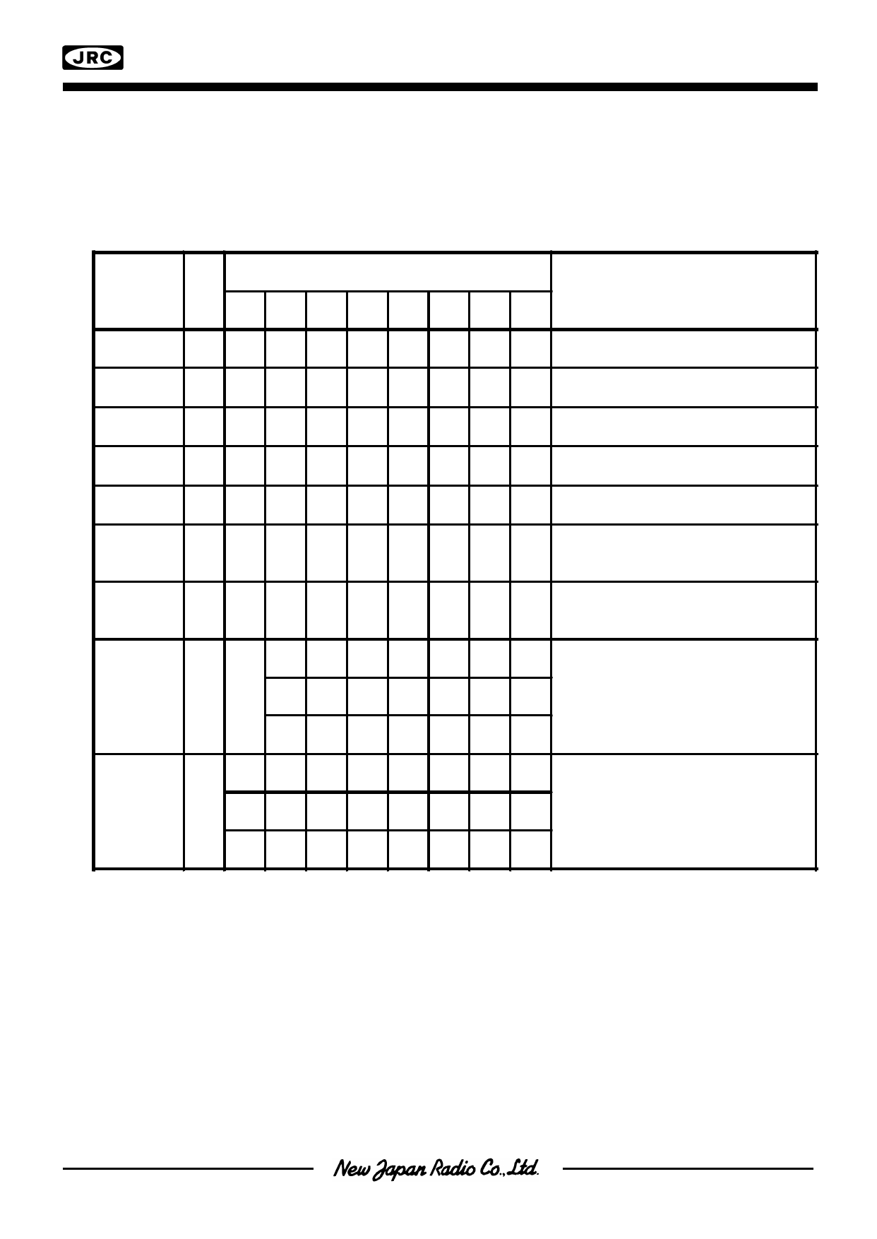
(3)Instruction
Each instruction is shown in the Table 3. The data should be written to the RAM continuously after the RAM
address set. The order of data writing is MSB first.
Table 3. Table of Instruction
MSB
Serial Data
LSB
INSTRUCTION
RS B7 B6 B5 B4 B3 B2 B1 B0
DESCRIPTION
Maker Test
000000 000
Output Port
Set
0 0 0 0 0 0 0 1 P1 Output Port Control
Display On/Off 0 0 0 0 0 0 1 M D Set the Display On/Off (Character and Icon)
Display
Duty Set
0
0
0
0
0
1 D2 D1 D0 Set the Contrast Control
Display Shift 0 0 0 0 1 0 LR M D Set the Display Shift (Character and Icon)
Display
Blink
Set
Display
Digits
Set
RAM
Address
Set
0 0 0 1 B2 B1 B0 M D Set the Blink Interval (Character and Icon)
0 0 1 0 0 0 C2 C1 C0 Set the Display Digits (9 to 16 degits)
0
0
0
AD3
AD2
AD1
AD0
Set the RAM Address
(AD0 to AD3 : DD RAM)
(AM0 to AM3 : MK RAM)
0
10
0
1 AM3 AM2 AM1 AM0 (AC0 to AC5 : CG RAM)
1 AC5 AC4 AC3 AC2 AC1 AC0
Write Data
to
RAM
SD7
SD6
SD5
SD4
SD3
SD2
SD1
SD0
After the RAM Address Set, the data should
be written to RAM
(SD0 to SD7 : DD RAM)
10
0
0
0
0
0 SM1 SM0 (SM0 to SM1 : MK RAM)
(SC0 to SC4 : CG RAM)
0 0 0 SC4 SC3 SC2 SC1 SC0
*Instruction is executed within 32uS from the rise edge of the Chip Select CS Signal. (at fOSC=250kHz)
Share Link: