MTP10N10E データシートの表示(PDF) - ON Semiconductor
部品番号
コンポーネント説明
メーカー
MTP10N10E Datasheet PDF : 8 Pages
| |||
MTP10N10E
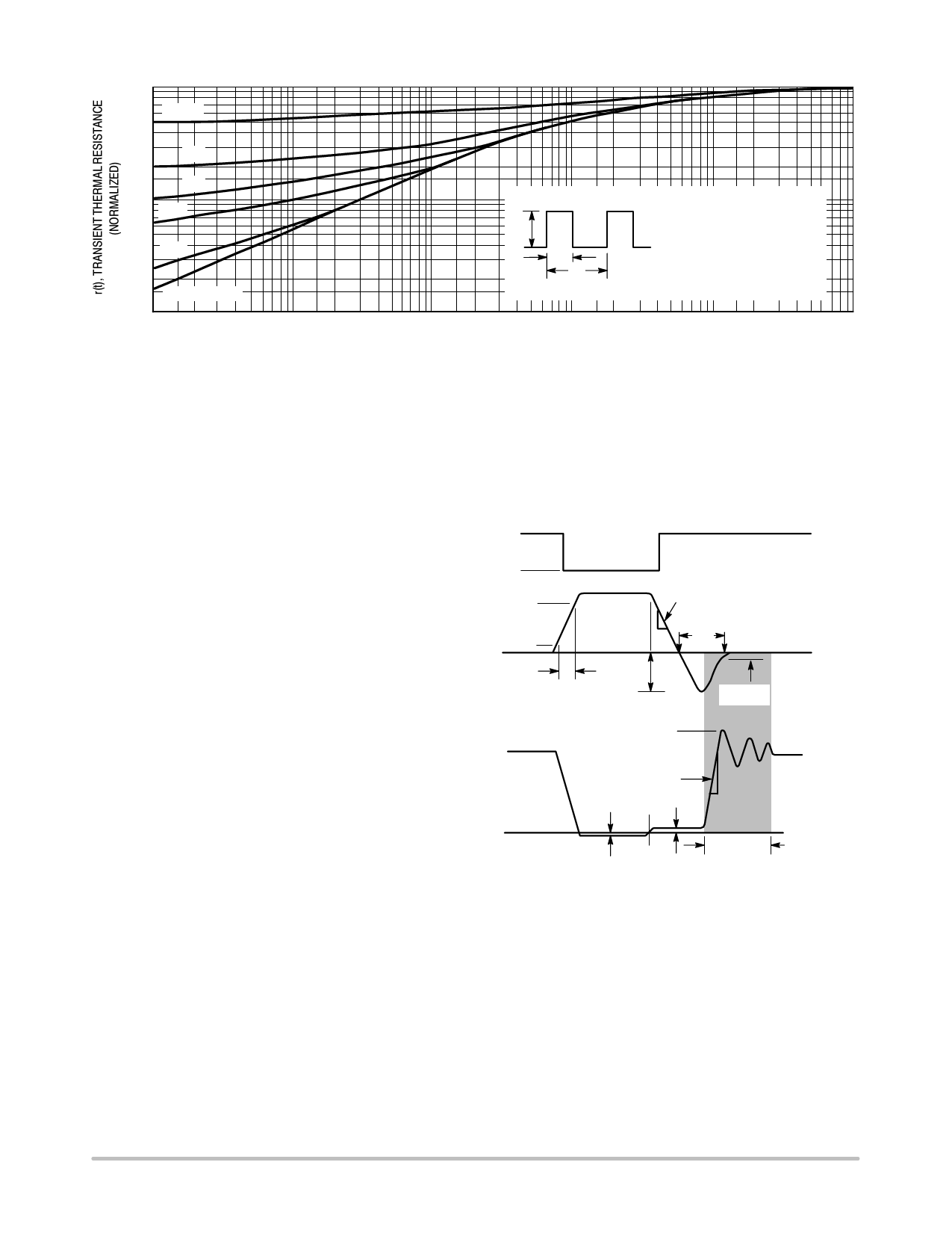
1
0.7
0.5
D = 0.5
0.3
0.2
0.2
0.1
0.1
0.07 0.05
0.05
0.01
0.03
0.02
SINGLE PULSE
0.01
0.01 0.02 0.03 0.05 0.1
P(pk)
t1
t2
DUTY CYCLE, D = t1/t2
RθJC(t) = r(t) RθJC
RθJC = 1.67°C/W MAX
D CURVES APPLY FOR POWER
PULSE TRAIN SHOWN
READ TIME AT t1
TJ(pk) - TC = P(pk) RθJC(t)
0.2 0.3 0.5 1
23 5
10
20 30 50
t, TIME (ms)
Figure 10. Thermal Response
100 200 300 500 100
COMMUTATING SAFE OPERATING AREA (CSOA)
The Commutating Safe Operating Area (CSOA) of Figure
12 defines the limits of safe operation for commutated
source-drain current versus re-applied drain voltage when
the source-drain diode has undergone forward bias. The
curve shows the limitations of IFM and peak VDS for a given
rate of change of source current. It is applicable when
waveforms similar to those of Figure 11 are present. Full or
half-bridge PWM DC motor controllers are common
applications requiring CSOA data.
Device stresses increase with increasing rate of change of
source current so dIs/dt is specified with a maximum value.
Higher values of dIs/dt require an appropriate derating of
IFM, peak VDS or both. Ultimately dIs/dt is limited primarily
by device, package, and circuit impedances. Maximum
device stress occurs during trr as the diode goes from
conduction to reverse blocking.
VDS(pk) is the peak drain–to–source voltage that the
device must sustain during commutation; IFM is the
maximum forward source-drain diode current just prior to
the onset of commutation.
VR is specified at 80% of V(BR)DSS to ensure that the
CSOA stress is maximized as IS decays from IRM to zero.
RGS should be minimized during commutation. TJ has
only a second order effect on CSOA.
Stray inductances in ON Semiconductor’s test circuit are
assumed to be practical minimums. dVDS/dt in excess of 10
V/ns was attained with dIs/dt of 400 A/µs.
15 V
VGS
0
90%
IS
10%
IFM
dls/dt
trr
ton
IRM
0.25 IRM
VDS(pk)
VR
VDS
dVDS/dt
Vf
VdsL
MAX. CSOA
STRESS
AREA
Figure 11. Commutating Waveforms
http://onsemi.com
5
Share Link: 