PD5036 データシートの表示(PDF) - Unspecified
部品番号
コンポーネント説明
メーカー
PD5036 Datasheet PDF : 14 Pages
| |||
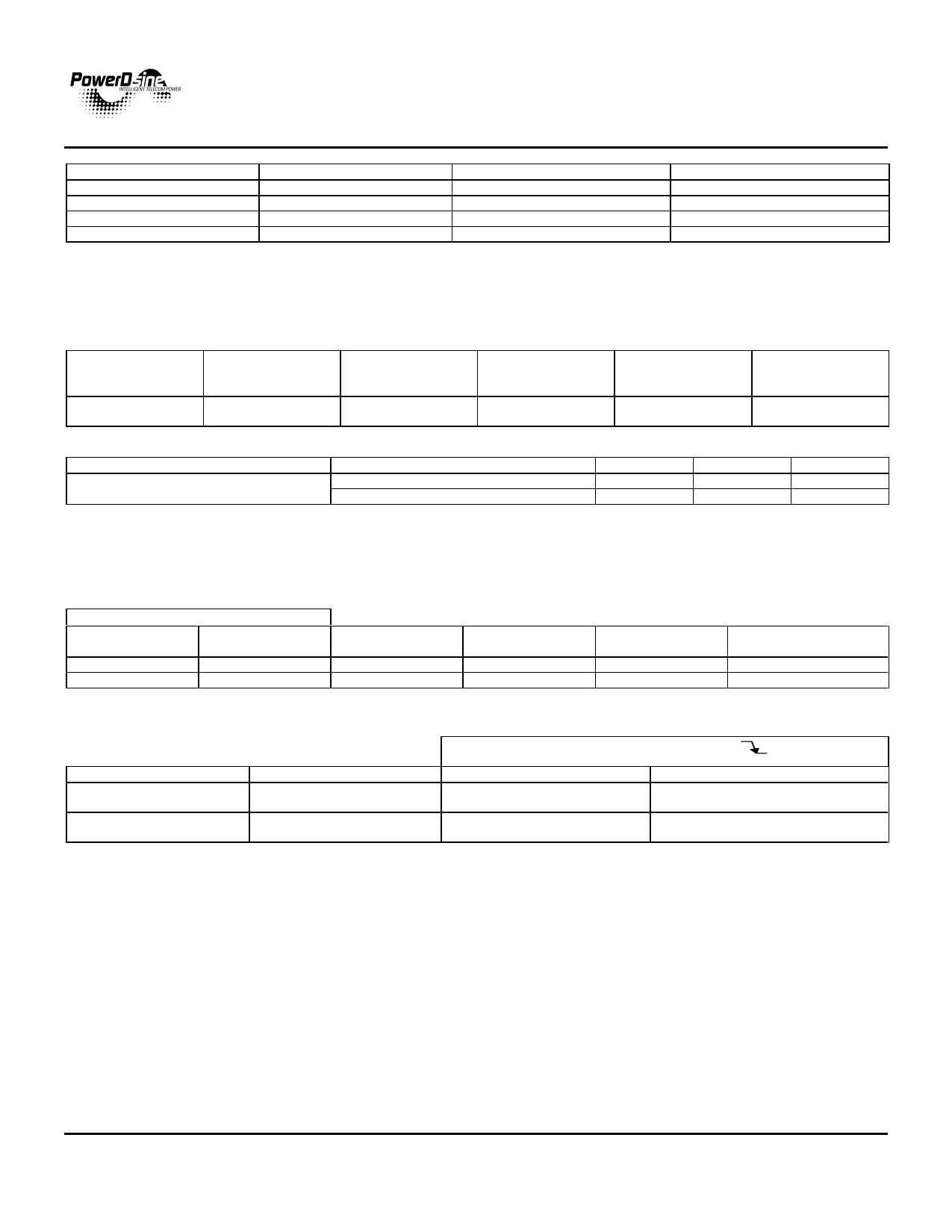
SYNC OUTPUT
F1
00
01
10
11
PD5036
TELEPHONE RING GENERATOR CONTROLLER
F0
Output Frequency
SYNC Pulse Width mS
50
4
16.7
5
25
5
20
5
INPUT VOLTAGE SAMPLING A/D CONVERTER
Unless otherwise stated, these specifications apply for: Vcc = +5V, -40C° ≤ TA ≤ +85°C, PAD_Out current ≤ 3mA.
INTERNAL FUNCTIONAL PARAMETERS
Main Clock
A/D
Resolution
19.66MHz
8 bit
12.28MHz
8 bit
A/D PWM
Frequency
PAD_Out
76.77KHz
47.97KHz
CAD_In
Sampling
Rate
9.6KHz
6.0KHz
Vsample Sensitivity
58.6mV
58.6mV
A/D BEHAVIORAL PARAMETERS
Symbol Param
eters
Min
A/D input operation voltage
Normal A/D operation
0.332
(Vsample)
A/D not used*
0
*CAD_In = “0” AND THE A/D REACHED ITS MINIMUM OPERATION VALUE (Minimum A/D Duty Cycle).
Max
4.98
0.293
Full Scale
Response
Time
24.89mS
39.83mS
Units
Vdc
Vdc
PWM UNIT
OPERATING RANGE
CL Input = ‘1’
Main Clock
FS
Output
PWM
PWM Frequency
Resolution
12.28MHz
0
96KHz
7 bit
19.66MHz
1
307.2KHz
6 bit
*Duty Cycle = Ratio between the time the signal’s On duration to the On + Off duration.
PWM
Duty Cycle * Min
0%
0%
PWM
Duty Cycle * Max
92.18%
92.18%
PWM UNIT OPERATION AT OVERLOAD CONDITION
PWM Turn Off Delay When
CL
FS M
ain Clock
0 12.
28Mhz
1
19.66Mhz
PWM Turn Off Delay When CL
Min
1 Main Clock
81.43ns
1 Main Clock
50.86ns
Max
2 Main Clocks
162.86ns
2 Main Clocks
101.72ns
PD5036
US Patent No. 5,828,558
Patent Pending in Europe and Asia
Share Link: 