AT93C56A データシートの表示(PDF) - Atmel Corporation
部品番号
コンポーネント説明
メーカー
AT93C56A Datasheet PDF : 14 Pages
| |||
Timing Diagrams
WRITE (WRITE): The Write (WRITE) instruction contains the 8 or 16 bits of data to be
written into the specified memory location. The self-timed programming cycle, tWP, starts
after the last bit of data is received at serial data input pin DI. The DO pin outputs the
Ready/Busy status of the part if CS is brought high after being kept low for a minimum of
250 ns (tCS). A logic “0” at DO indicates that programming is still in progress. A logic “1”
indicates that the memory location at the specified address has been written with the
data pattern contained in the instruction and the part is ready for further instructions. A
Ready/Busy status cannot be obtained if the CS is brought high after the end of the self-
timed programming cycle, tWP.
ERASE ALL (ERAL): The Erase All (ERAL) instruction programs every bit in the mem-
ory array to the logic “1” state and is primarily used for testing purposes. The DO pin
outputs the ready/busy status of the part if CS is brought high after being kept low for a
minimum of 250 ns (tCS). The ERAL instruction is valid only at VCC = 5.0V ± 10%.
WRITE ALL (WRAL): The Write All (WRAL) instruction programs all memory locations
with the data patterns specified in the instruction. The DO pin outputs the Ready/Busy
status of the part if CS is brought high after being kept low for a minimum of 250 ns (tCS).
The WRAL instruction is valid only at VCC = 5.0V ± 10%.
ERASE/WRITE DISABLE (EWDS): To protect against accidental data disturb, the
Erase/Write Disable (EWDS) instruction disables all programming modes and should be
executed after all programming operations. The operation of the Read instruction is
independent of both the EWEN and EWDS instructions and can be executed at any
time.
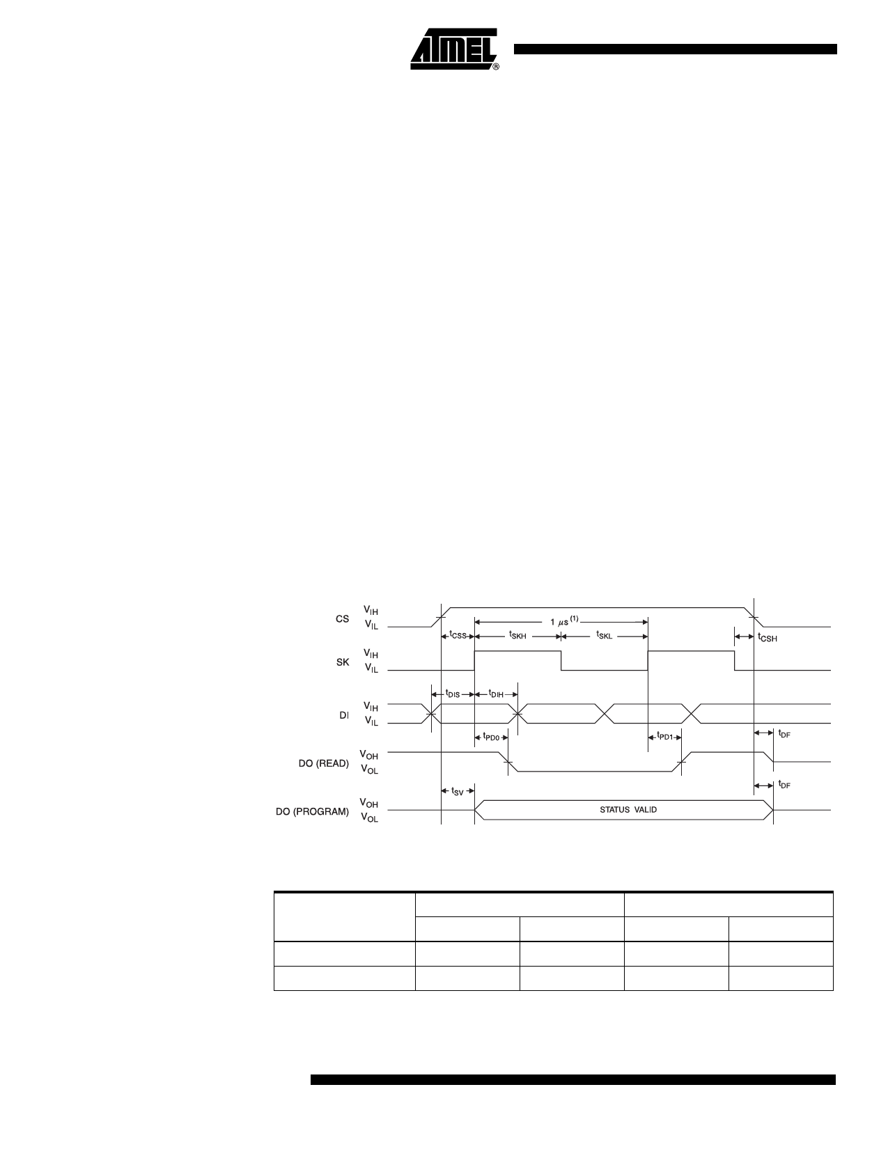
Figure 1. Synchronous Data Timing
Note: This is the minimum SK period.
Table 5. Organization Key for Timing Diagrams
AT93C56A (2K)
AT93C66A (4K)
I/O
x8
x 16
x8
AN
A8(1)
A7(2)
A8
DN
D7
D15
D7
Notes: 1. A8 is a don’t care value, but the extra clock is required.
2. A7 is a don’t care value, but the extra clock is required.
x 16
A7
D15
6 AT93C56A/66A
5091D–SEEPR–2/07
Share Link: 