INF8574 データシートの表示(PDF) - IK Semicon Co., Ltd
部品番号
コンポーネント説明
メーカー
INF8574 Datasheet PDF : 11 Pages
| |||
INF8574
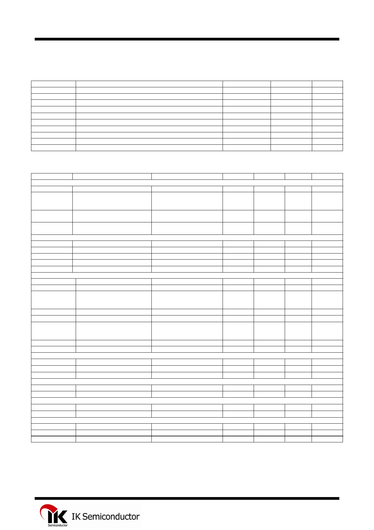
LIMITING VALUES
SYMBOL
PARAMETER
VDD
supply voltage
VI
input voltage
II
DC input current
IO
DC output current
IDD
supply current
ISS
supply current
Ptot
total power dissipation
PO
power dissipation per output
Tstg
storage temperature
Tamb
operating ambient temperature
MIN.
-0.5
VSS - 0.5
-
-
-
-
-
-
65
40
MAX.
+7.0
VDD + 0.5
±20
±25
±100
±100
400
100
+150
+85
UNIT
V
V
mA
mA
mA
mA
mW
mW
oC
oC
DC CHARACTERISTICS VDD = 2.5 to 6 V; VSS = 0 V; Tamb =40 to +85 oC; unless otherwise specified.
SYMBOL
PARAMETER
CONDITIONS
MIN.
TYP.
MAX.
UNIT
Supply
VDD
supply voltage
IDD
supply current
Istb
standby current
VPOR
power-on reset voltage
Input SCL; input/output SDA
2.5
6.0
V
operating mode; VDD = 6 V;
no load; VI = VDD or VSS;
40
100
µA
fSCL = 100 kHz
standby mode; VDD = 6 V;
no load; VI = VDD or VSS
2.5
10
µA
VDD = 6 V; no load;
1.3
2.4
V
VI = VDD or VSS; note 1
VIL
VIH
IOL
|IL|
CI
I/O Ports
LOW level input voltage
HIGH level input voltage
LOW level output current
leakage current
input capacitance
VOL = 0.4 V
VI = VDD or VSS
VI = VSS
-0.5
0.7VDD
3
+0.3VDD V
VDD + 0.5 V
mA
1
µA
7
pF
VIL
VIH
IIHL(max)
LOW level input voltage
HIGH level input voltage
maximum allowed input
current through protection
VI ≥VDD or VI≤ VSS
-0.5
-0.7VDD
+0.3VDD V
VDD + 0.5 V
±400
µA
diode
IOL
LOW level output current
VOL = 1 V; VDD = 5 V
10
25
mA
IOH
HIGH level output current
VOH = VSS
30
300
µA
IOHt
transient pull-up current
HIGH during acknowledge
mA
(see Fig.14); VOH = VSS;
1
VDD = 2.5 V
CI
input capacitance
10
pF
CO
output capacitance
10
pF
Port timing CL ≤100 pF
tpv
output data valid
4
µs
tsu
input data set-up time
0
µs
th
input data hold time
4
µs
Interrupt INT
IOL
LOW level output current
VOL = 0.4 V
1.6
|IL|
leakage current
VI = VDD or VSS
Timing; CL ≤100 pF
tiv
input data valid time
tir
reset delay time
mA
1
µA
4
µs
4
µs
Select inputs A0 to A2
VIL
VIH
|ILI|
Note
LOW level input voltage
HIGH level input voltage
input leakage current
pin at VDD or VSS
-0.5
0.7VDD
+0.3VDD V
VDD + 0.5 V
250
nA
1. The power-on reset circuit resets the I2C-bus logic with VDD < VPOR and sets all Ports to logic 1 (with current
source to VDD).
9
Share Link: 