2SK3652 データシートの表示(PDF) - Panasonic Corporation
部品番号
コンポーネント説明
メーカー
2SK3652 Datasheet PDF : 4 Pages
| |||
Power MOSFETs
2SK3652
N-channel enhancement mode MOSFET
■ Features
• Low on-resistance, low Qg
• High avalanche resistance
■ Applications
• For PDP
• For high-speed switching
■ Absolute Maximum Ratings TC = 25°C
Parameter
Symbol Rating
Unit
Drain-source surrender voltage
Gate-source surrender voltage
Drain current
Peak drain current
Avalanche energy capability *
VDSS
230
V
VGSS
±30
V
ID
50
A
IDP
200
A
EAS
2 200
mJ
Power dissipation
Junction temperature
Storage temperature
PD
100
W
Ta = 25°C
3
Tj
150
°C
Tstg −55 to +150 °C
Note) *: L = 1 mH, IL = 50 A, VDD = 100 V, 1 pulse, Ta = 25°C
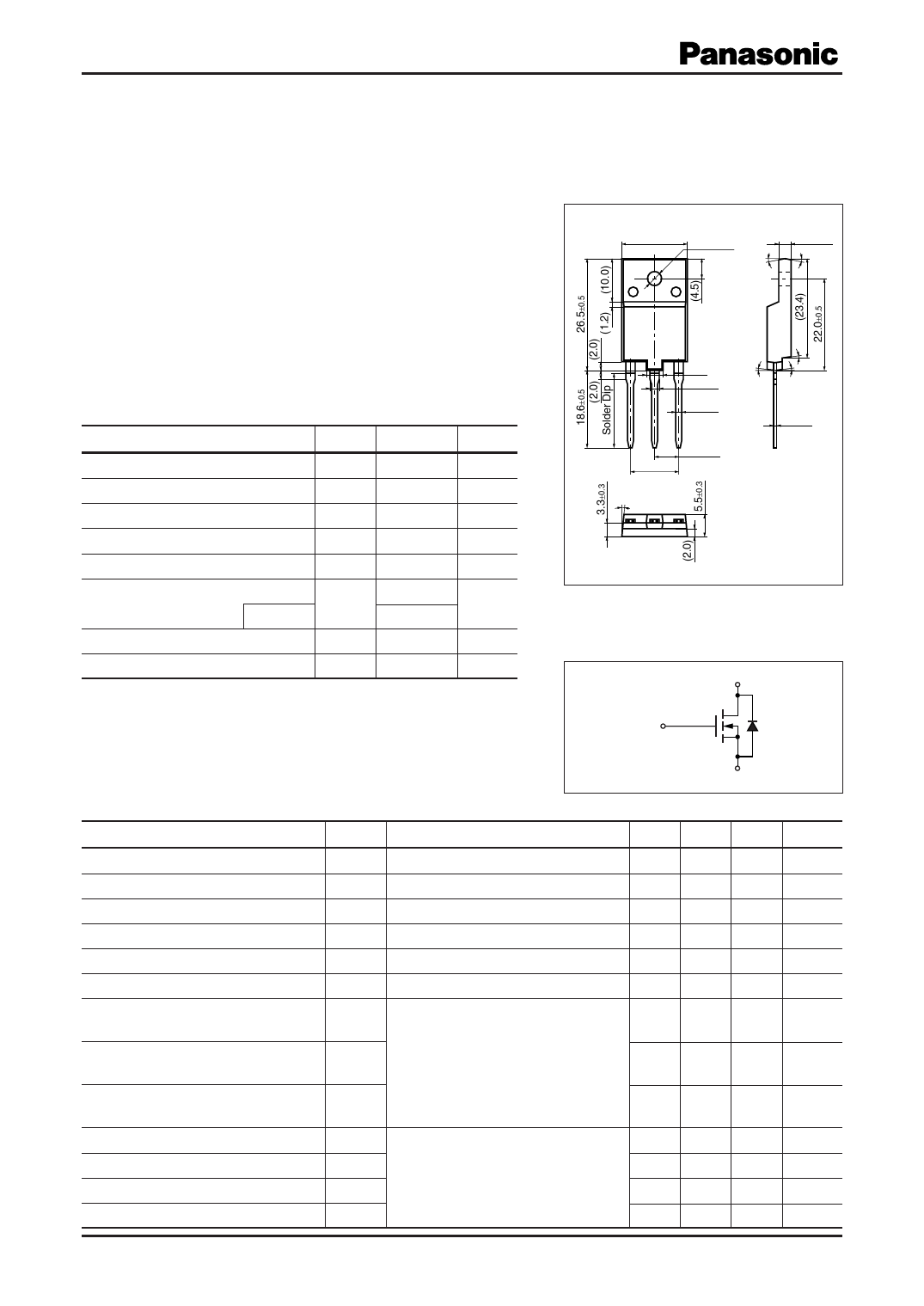
15.5±0.5 φ 3.2±0.1
Unit: mm
3.0±0.3
5˚
5˚
5˚
(4.0)
5˚
2.0±0.2
5˚
1.1±0.1
0.7±0.1
5.45±0.3
10.9±0.5
5˚
12 3
1: Gate
2: Drain
3: Source
TOP-3E-A1 Package
Marking Symbol: K3652
Internal Connection
D
G
■ Electrical Characteristics TC = 25°C ± 3°C
Parameter
Symbol
Conditions
Drain-source surrender voltage
VDSS
Gate threshold voltage
Vth
Drain-source cutoff current
IDSS
Gate-source cutoff current
IGSS
Drain-source ON resistance
RDS(on)
Forward transfer admittance
Yfs
Short-circuit forward transfer capacitance Ciss
(Common-source)
ID = 1 mA, VGS = 0
VDS = 25 V, ID = 10 mA
VDS = 184 V, VGS = 0
VGS = ±30 V, VDS = 0
VGS = 10 V, ID = 25 A
VDS = 25 V, ID = 25 A
VDS = 25 V, VGS = 0, f = 1 MHz
Short-circuit output capacitance
Coss
(Common-source)
Reverse transfer capacitance
Crss
(Common-source)
Turn-on delay time
Rise time
Turn-off delay time
Fall time
td(on)
Tr
td(off)
tf
VDD = 100 V, ID = 25 A
RL = 4 Ω, VGS = 10 V
Publication date: March 2004
SJG00034AED
S
Min Typ Max Unit
230
V
2
4
V
100 µA
±1
µA
29
40
mΩ
17 35
S
5 950
pF
850
pF
80
pF
65
ns
140
ns
470
ns
145
ns
1
Share Link: 