ADT7476AARQZ データシートの表示(PDF) - ON Semiconductor
部品番号
コンポーネント説明
メーカー
ADT7476AARQZ Datasheet PDF : 67 Pages
| |||
ADT7476A
Table 5 shows the input ranges of the analog inputs and
output codes of the 10-bit ADC.
When the ADC is running, it samples and converts a
voltage input in 0.7 ms and averages 16 conversions to
reduce noise; a measurement takes nominally 11 ms.
Extended Resolution Registers
Voltage measurements can be made with higher accuracy
using the extended resolution registers (0x76 and 0x77).
Whenever the extended resolution registers are read, the
corresponding data in the voltage measurement registers
(0x20 to 0x24) is locked until their data is read. That is, if
extended resolution is required, then the extended resolution
register must be read first, immediately followed by the
appropriate voltage measurement register.
Additional ADC Functions for Voltage Measurements
A number of other functions are available on the
ADT7476A to offer the system designer increased
flexibility.
Turn-Off Averaging
For each voltage/temperature measurement read from a
value register, 16 readings have been made internally and the
results averaged before being placed into the value register.
When faster conversions are needed, setting Bit 4 of
Configuration Register 2 (0x73) turns averaging off. This
effectively gives a reading 16 times faster but the reading
can be noisier. The default round robin cycle time takes
146.5 ms.
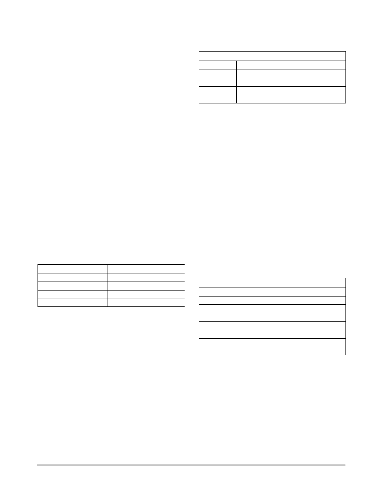
Table 2. Conversion Time with Averaging Disabled
Channel
Voltage Channels
Remote Temperature 1
Remote Temperature 2
Local Temperature
Measurement Time (ms)
0.7
7
7
1.3
When Bit 7 of Configuration Register 6 (0x10) is set, the
default round robin cycle time increases to 240 ms.
Bypass All Voltage Input Attenuators
Setting Bit 5 of Configuration Register 2 (0x73) removes
the attenuation circuitry from the 2.5 V, VCCP, VCC, 5.0 V, and
12 V inputs. This allows the user to directly connect external
sensors or rescale the analog voltage measurement inputs for
other applications. The input range of the ADC without the
attenuators is 0 V to 2.25 V.
Bypass Individual Voltage Input Attenuators
Bits [7:4] of Configuration Register 4 (0x7D) can be used
to bypass individual voltage channel attenuators.
Table 3. Bypassing Individual Voltage Input
Attenuators
Configuration Register 4 (0x7D)
Bit No.
4
5
6
7
Channel Attenuated
Bypass 2.5 V attenuator
Bypass VCCP attenuator
Bypass 5.0 V attenuator
Bypass 12 V attenuator
Configuration Register 2 (0x73)
[4] = 1, averaging off.
[5] = 1, bypass input attenuators.
[6] = 1, single-channel convert mode.
TACH1 Minimum High Byte (0x55)
[7:5] Selects ADC channel for single-channel convert mode.
Single-Channel ADC Conversion
While single-channel mode is intended as a test mode that
can be used to increase sampling times for a specific
channel, and therefore helps to analyze that channel’s
performance in greater detail, it can also have other
applications.
Setting Bit 6 of Configuration Register 2 (0x73) places the
ADT7476A into single-channel ADC conversion mode. In
this mode, the ADT7476A can only read a single voltage
channel. The selected voltage input is read every 0.7 ms. The
appropriate ADC channel is selected by writing to Bits [7:5]
of the TACH1 minimum high byte register (0x55).
Table 4. Programming Single‚àíChannel ADC Mode
Bits [7:4], Register 0x55
Channel Selected (Note 1)
000
2.5 V
001
VCCP
010
VCC
011
5.0 V
100
12 V
101
Remote 1 temperature
110
Local temperature
111
Remote 2 temperature
1. In the process of configuring single-channel ADC conversion
mode, the TACH1 minimum high byte is also changed, possibly
trading off TACH1 minimum high byte functionality with
single-channel mode functionality.
http://onsemi.com
14
Share Link: 