UPB1505GR データシートの表示(PDF) - NEC => Renesas Technology
部品番号
コンポーネント説明
メーカー
UPB1505GR Datasheet PDF : 8 Pages
| |||
µPB1505GR
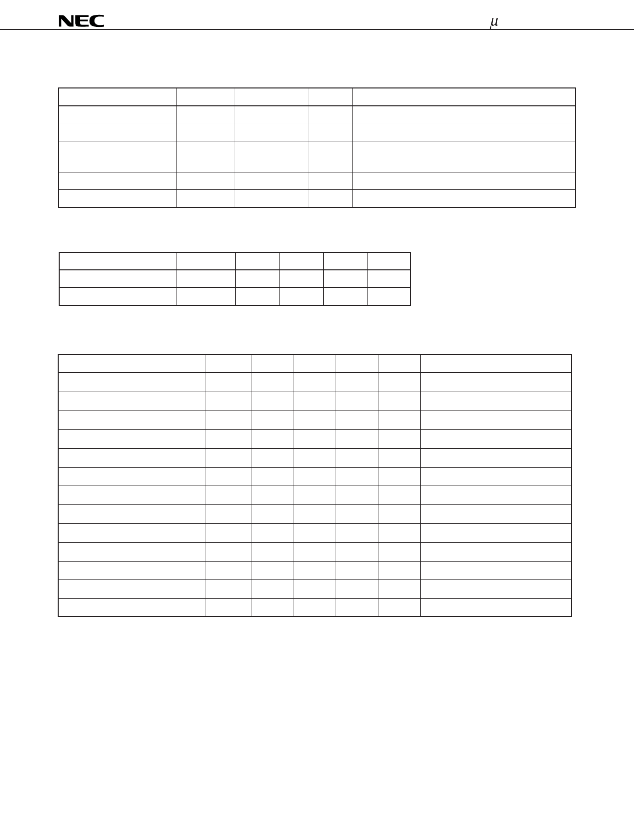
ABSOLUTE MAXIMUM RATINGS
PARAMETER
Supply voltage
Input voltage
Power dissipation
Operating temperature
Storage temperature
SYMBOL
VCC
VIN
PD
Topt
Tstg
RATING
–0.5 to +6
–0.5 to VCC +0.5
250
–40 to +85
–55 to +150
UNIT
V
V
mW
°C
°C
CONDITIONS
TA = +25 °C
TA = +25 °C
Mounted on 50 × 50 × 1.6 mm double copper clad
epoxy glass PWB (TA = +85 °C)
RECOMMENDED OPERATING RANGE
PARAMETER
Supply voltage
Operating temperature
SYMBOL
VCC
Topt
MIN.
4.5
–40
TYP.
5.0
+25
MAX.
5.5
+85
UNIT
V
°C
ELECTRICAL CHARACTERISTICS (TA = –40 to +85 °C, VCC = 4.5 to 5.5 V)
PARAMETER
Circuit current
Upper response frequency 1
Upper response frequency 2
Lower response frequency 1
Lower response frequency 2
Input sensitivity 1
Input sensitivity 2
Input sensitivity 3
Output Swing
SW1 input voltage (H)
SW1 input voltage (L)
SW2 input voltage (H)
SW2 input voltage (L)
SYMBOL
ICC
fin(U)1
fin(U)2
fin(L)1
fin(L)2
Pin1
Pin2
Pin3
VOUT
VIH1
VIL1
VIH2
VIL2
MIN.
9.0
3.0
2.7
–10
–14
–10
1.3
VCC
OPEN
VCC
OPEN
TYP.
14.0
1.6
VCC
OPEN
VCC
OPEN
MAX.
19.5
0.5
1.0
+8
+10
+10
VCC
OPEN
VCC
OPEN
UNIT
mA
GHz
GHz
GHz
GHz
dBm
dBm
dBm
VP-P
V
V
V
V
CONDITIONS
No input signal
Pin = –10 to +10 dBm
Pin = –14 to –10 dBm
Pin = –10 to +8 dBm
Pin = –14 to –10 dBm, +8 to +10 dBm
fin = 0.5 to 1.0 GHz
fin = 1.0 to 2.7 GHz
fin = 2.7 to 3.0 GHz
CL = 8 pF
Data Sheet P10872EJ3V0DS00
3
Share Link: 