M66510 データシートの表示(PDF) - MITSUBISHI ELECTRIC
部品番号
コンポーネント説明
メーカー
M66510 Datasheet PDF : 10 Pages
| |||
MITSUBISHI 〈DIGITAL ASSP〉
M66510P/FP
LASER-DIODE DRIVER
DESCRIPTION OF OPERATION
1. Setting laser driving current
The M66510 is provided internally with three constant current
sources IL1, IL2 and IL3, allowing setting of each independent
output current.
The methods of setting IL1 to IL3 are given below in (1) to (3).
(1) Method of setting IL1
IL1 is approximated by the VL1 pin input voltage and the re-
sistor (RC1) connected between 1RC pin and GND as fol-
lows:
IL1[mA] = 12 ×
VL1[V]
RC1[kΩ]
However, 0 ≤ VL1 ≤ VCC – 1.8V, IL1(max.) = 60mA
(2) Method of setting IL2
IL2 is approximated by the VL2 pin input voltage and the re-
sistor (RC2) connected between 2RC pin and GND as fol-
lows:
IL2[mA]
=
6
×
VL2[V]
RC2[kΩ]
However, 0 ≤ VL2 ≤ Vcc – 1.8V, IL2(max.) = 30mA
(3) Method of setting IL3
IL3 is approximated by the internal reference voltage (Vref)
and the resistor (RC3) connected between 3RC pin and GND
as follows:
IL3[mA] = 10 ×
Vref[V]
RC3[kΩ]
However, Vref = 1.2V (standard), IL3(max.) = 30mA
Note: The expressions for setting IL1 to IL3 are typical. Actually, the set values
fluctuate several % depending on IC lot dispersion or operating ambient
temperature (See the ELECTRICAL CHARACTERISTICS).
2. Switching operation
The laser is turned on when DATA = “L”. At this time, the la-
ser driving current is IL1 + IL2 + IL3.
The laser is turned off when DATA = “H”. At this time, the la-
ser driving current becomes almost 0 regardless of IL1 to IL3.
3. Usage of VOFF input
The current which flows into the laser becomes 0 when
DATA = “H”. And the laser is turned off but the internal cur-
rent sources are active.
Contrarily, the internal current sources are turned off when
VOFF = “L”. It is therefore possible to prevent overcurrent from
flowing into the laser by setting VOFF input to “L” until VCC
reaches 3.5V (standard) at the power-ON time, for example
(See 6. Internal reset).
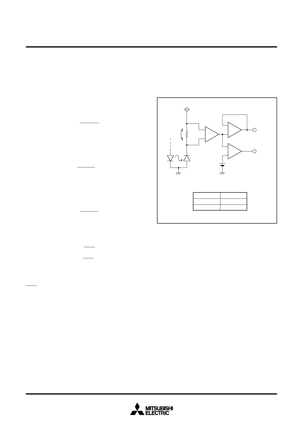
4. Laser power monitor operation
The M66510 outputs the information on monitor photodiode
(PD) built in the laser from the MO and CO pins in the flow
given below.
(1) The current equal to the PD current produced through
emission of the laser flows into the resistor (RM) connected
between 1RM and 2RM. The potential difference (VM) pro-
duced on RM is converted into a level from GND by the inter-
nal differential amplifier.
(2) The VM is output as an analog output from the MO pin
through the buffer amplifier and compared to the internal ref-
erence voltage Vref (1.2V standard) by the comparator. Then
the result of comparison is output from the CO pin on the TTL
level.
VM
LD
+
RM
–
Differential
amplifier
PD
Vref
–
+
Buffer
amplifier
MO output
+
CO output
–
Comparator
Condition
VM < Vref
VM > Vref
CO output
“L”
“H”
Monitor circuit schematic drawing
3
Share Link: 