TP2640N3 データシートの表示(PDF) - Supertex Inc
部品番号
コンポーネント説明
メーカー
TP2640N3 Datasheet PDF : 4 Pages
| |||
TP2635/TP2640
Thermal Characteristics
Package
SO-8
ID (continuous)1 ID (pulsed)
-210mA
-1.25A
Power Dissipation
@TC = 25OC
1.3W2
Θjc (OC/W)
24
Θjc (OC/W)
962
IDR1
210mA
IDRM
-1.25A
TO-92
-180mA
-0.8A
Notes:
1. ID (continuous) is limited by max rated Tj.
2. Mounted on FR4 board, 25mm x 25mm x 1.57mm
1.0W
125
170
-180mA
-0.8A
Electrical Characteristics (TJ = 25°C unless otherwise specified)
Symbol Parameter
Min
Typ
Max
Units Conditions
BVDSS
Drain-to-source break-
down voltage
TP2640
TP2635
-400
-350
-
-
V
VGS = 0V, ID = -2.0mA
VGS(th) Gate threshold voltage
-0.8
-
-2.0
V
VGS = VDS, ID = -1.0mA
ΔVGS(th) Change in VGS(th) with temperature
-
-
5
mV/OC VGS = VDS, ID = -1.0mA
IGSS Gate body leakage
-
-100
nA VGS = ±20V, VDS = 0V
-1.0
µA VDS = -100V, VGS = 0V
IDSS Zero gate voltage drain current
-
-
-10.0
µA VDS = Max rating, VGS = 0V
-1.0
mA
VDS = 0.8 Max Rating,
VGS = 0V, TA = 125OC
ID(ON) ON-state drain current
0.7
-
-
A
VGS = -10V, VDS = -25V
RDS(ON)
Static drain-to-source ON-state
resistance
12
15
-
11
15
11
15
VGS = -2.5V, ID = -200mA
Ω
VGS = -4.5V, ID = -150mA
VGS = -10V, ID = -300mA
ΔRDS(ON) Change in RDS(ON) with temperature
-
-
0.75 %/OC VGS = -10V, ID = -300mA
GFS Forward transconductance
200
-
-
m
VDS = -25V, ID = -300mA
CISS Input capacitance
-
-
300
COSS Common source output capacitance
-
-
50
pF VGS = 0V, VDS = -25V, f = 1MHz
CRSS Reverse transfer capacitance
-
-
12
td(ON) Turn-ON delay time
-
-
10
tr
td(OFF)
Rise time
Turn-OFF delay time
-
-
-
15
-
60
ns
VDD = 25V, ID = 2.0A,
RGEN = 25Ω
tf
Fall time
-
-
40
VSD Diode forward voltage drop
-
-
-1.8
V
VGS = 0V, ISD = 200mA
trr
Reverse recovery time
-
300
-
ns
VGS = 0V, ISD = 1.0A
Notes:
1.All D.C. parameters 100% tested at 25C unless otherwise stated. (Pulse test: 300s pulse, 2% duty cycle.)
2.All A.C. parameters sample tested.
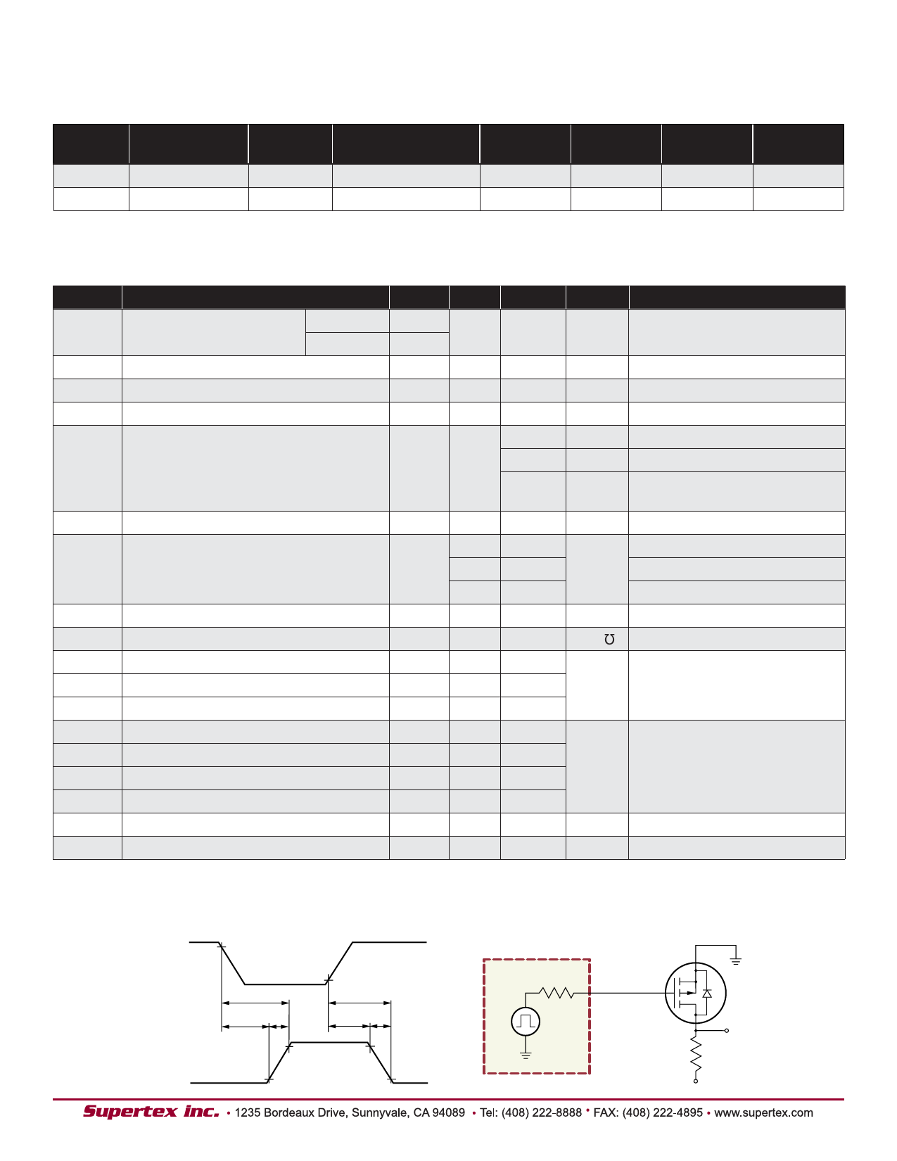
N- Channel Switching Waveforms and Test Circuit
0V
INPUT
10%
PULSE
GENERATOR
-10V
t(ON)
90%
t(OFF)
Rgen
0V
OUTPUT
VDD
td(ON)
tr
td(OFF)
tF
90%
90%
10%
10%
INPUT
D.U.T.
OUTPUT
RL
VDD
2
Share Link: 