MAX4621CSE データシートの表示(PDF) - Maxim Integrated
部品番号
コンポーネント説明
メーカー
MAX4621CSE Datasheet PDF : 12 Pages
| |||
Dual, 5Ω Analog Switches
PIN
MAX4621
1, 8
2–7
9, 16
10, 15
11
12
13
14
MAX4622
1, 3, 6, 8
2, 7
4, 5, 9, 16
10, 15
11
12
13
14
MAX4623
1, 3, 6, 8
2, 7
4, 5, 9, 16
10, 15
11
12
13
14
NAME
Pin Description
FUNCTION
COM1,
COM2
N.C.
NO2, NO1
IN2, IN1
V+
VL
GND
V-
Switch Common Terminal
Not internally connected
Switch Normally Open
Terminal
Digital Logic Inputs
Positive Supply-Voltage Input
Logic Supply-Voltage Input
Ground
Negative Supply Voltage
Input
COM_
N.C.
NC_, NO_
IN2, IN1
V+
VL
GND
V-
Switch Common Terminal
Not internally connected
Switch Normally Closed/Open
Terminal
Digital Logic Inputs
Positive Supply-Voltage Input
Logic Supply-Voltage Input
Ground
Negative Supply Voltage
Input
COM_
N.C.
NO_
IN2, IN1
V+
VL
GND
V-
Switch Common Terminal
Not internally connected
Switch Normally Open
Terminal
Digital Logic Inputs
Positive Supply-Voltage Input
Logic Supply-Voltage Input
Ground
Negative Supply Voltage
Applications Information
Operation with Supply Voltages
Other than ±15V
The MAX4621/MAX4622/MAX4623 switches operate with
±4.5V to ±18V bipolar supplies and a +4.5V to +36V sin-
gle supply. In either case, analog signals ranging from
V+ to V- can be switched. The Typical Operating
Characteristics graphs show the typical on-resistance
variation with analog signal and supply voltage.
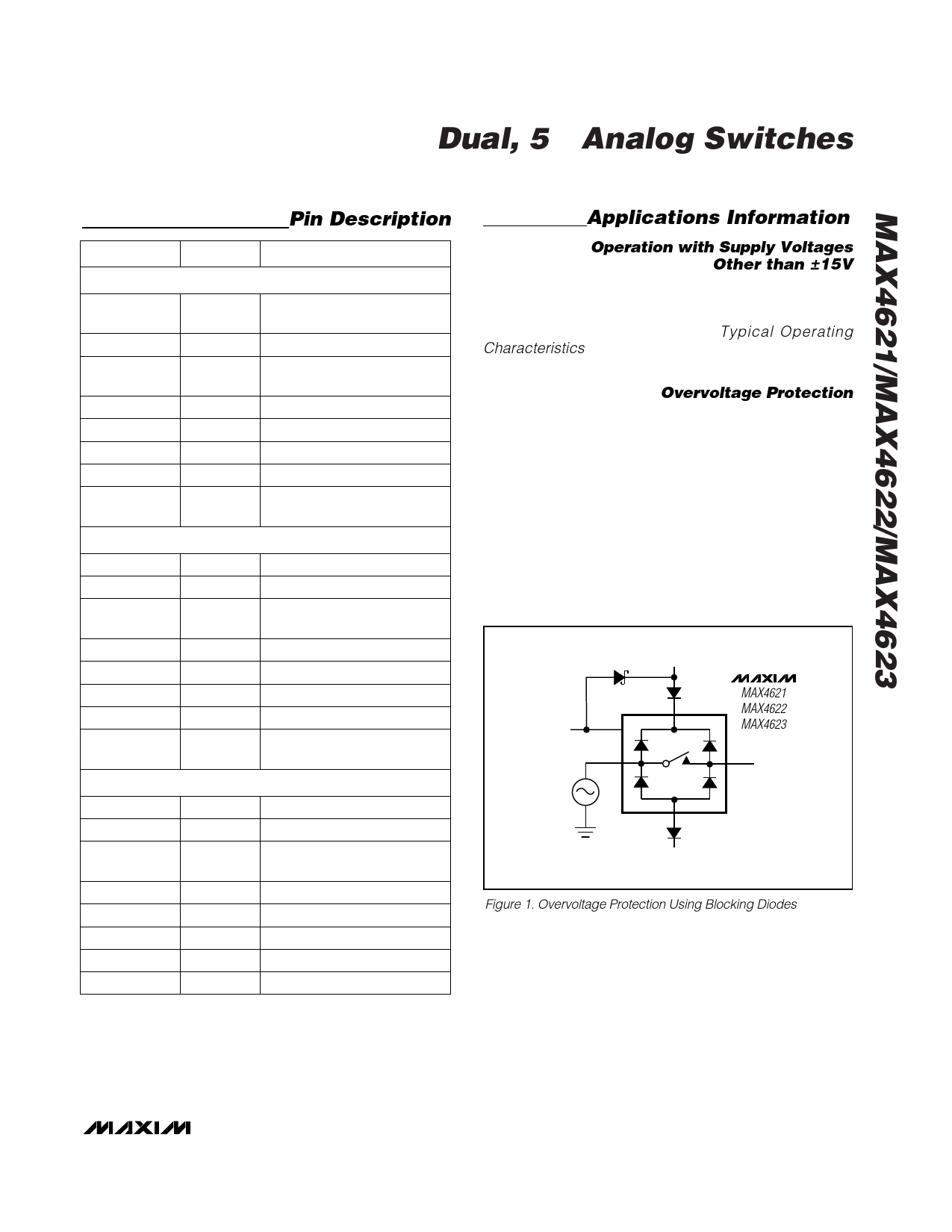
Overvoltage Protection
Proper power-supply sequencing is recommended for all
CMOS devices. It is important not to exceed the absolute
maximum ratings because stresses beyond the listed rat-
ings may cause permanent damage to the devices.
Always sequence V+ on first, followed by VL, V-, and
logic inputs. If power-supply sequencing is not possible,
add two small signal diodes in series with the supply pins
and a Schottky diode between V+ and VL (Figure 1).
Adding diodes reduces the analog signal range to 1V
below V+ and 1V above V-, but low switch resistance and
low leakage characteristics are unaffected. The differ-
ence between V+ and V- should not exceed +44V.
V+
VL
*
NO_
Vg
*
MAX4621
MAX4622
MAX4623
*
COM_
*
V-
*INTERNAL PROTECTION DIODES
Figure 1. Overvoltage Protection Using Blocking Diodes
_______________________________________________________________________________________ 7
Share Link: 