LB1929 データシートの表示(PDF) - ON Semiconductor
部品番号
コンポーネント説明
メーカー
LB1929
ON Semiconductor

LB1929 Datasheet PDF : 11 Pages
| |||
LB1929
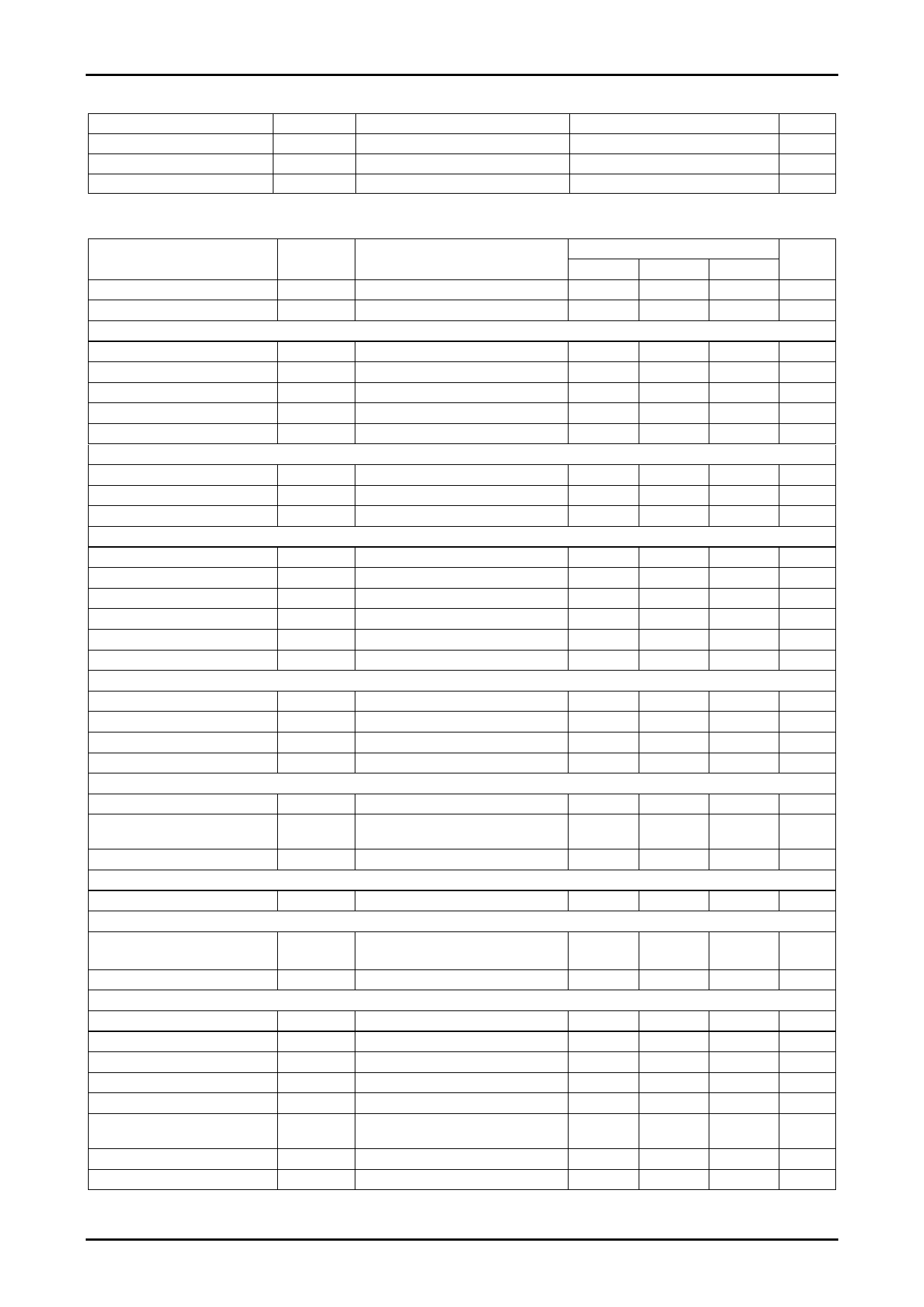
Allowable Operating Ranges at Ta = 25°C
Parameter
Symbol
Power supply voltage range 1
Regulator voltage output current
LD output current
VCC
IREG
ILD
Conditions
Ratings
Unit
9.5 to 28
V
0 to -30
mA
0 to 15
mA
Electrical Characteristics at Ta = 25°C, VCC = VM = 24V
Parameter
Symbol
Conditions
Power supply current 1
Power supply current 2
Output
ICC1
ICC2
In STOP mode
Output saturation voltage 1
Output saturation voltage 2
Output leak current
Lower-side diode forward voltage 1
Lower-side diode forward voltage 2
5V regulator voltage output
VOsat1
VOsat2
IOleak
VD1
VD2
IO = 1.0A, VO (SINK) +VO (SOURCE)
IO = 2.0A, VO (SINK) +VO (SOURCE)
ID = -1.0A
ID = -2.0A
Output voltage
Voltage fluctuation
Load fluctuation
Hall amplifier
VREG
ΔVREG1
ΔVREG2
IO = -5mA
VCC = 9.5 to 28V
IO = -5 to -20mA
Input bias current
Common mode input voltage range
IHB
VICM
Hall input sensitivity
Hysteresis width
Input voltage L→H
ΔVIN
VSLH
Input voltage H→L
VSHL
PWM oscillator
Output High level voltage
Output Low level voltage
Oscillator frequency
VOH (PWM)
VOL (PWM)
F (PWM)
C = 3900pF
Amplitude
V (PWM)
CSD circuit
Operating voltage
External capacitance charge
current
Operating time
VOH (CSD)
ICHG
T (CSD)
C = 10μF Design target value
Current limiter operation
Limiter
Thermal shutdown operation
VRF
VCC-VM
Thermal shutdown operating
temperature
TSD
Design target value (junction temperature)
Hysteresis width
ΔTSD
Design target value (junction temperature)
FG amplifier
Input offset voltage
Input bias current
Output High level voltage
Output Low level voltage
FG input sensitivity
VIO (FG)
IB (FG)
VOH (FG)
VOL (FG)
IFGO = -0.2mA
IFGO = 0.2mA
GAIN 100 times
Next-stage Schmitt comparator
width
Operation frequency range
Design target value*
Open-loop gain
f (FG) = 2kHz
Note*: These items are design target values and are not tested.
min
4.65
-2
1.5
80
15
2.5
1.2
1.05
3.6
-17
0.45
150
-10
-1
VREG-1.2
3
100
45
Ratings
typ
23
3.5
Unit
max
30
mA
5.0
mA
2.0
2.5
V
2.6
3.2
V
100
μA
1.2
1.5
V
1.5
2.0
V
5.00
5.35
V
30
100
mV
20
100
mV
-0.5
μA
VREG-1.5
V
mVp-p
24
42
mV
12
mV
-12
mV
2.8
3.1
V
1.5
1.8
V
18
kHz
1.30
1.55 Vp-p
3.9
4.2
V
-12
-9
μA
3.3
s
0.5
0.55
V
180
°C
50
°C
VREG-0.8
0.8
180
+10
mV
+1
μA
V
1.2
V
mV
250
mV
2 kHz
51
dB
Continued on next page.
No.7099-2/11
Share Link: