LB1929 データシートの表示(PDF) - ON Semiconductor
部品番号
コンポーネント説明
メーカー
LB1929
ON Semiconductor

LB1929 Datasheet PDF : 11 Pages
| |||
LB1929
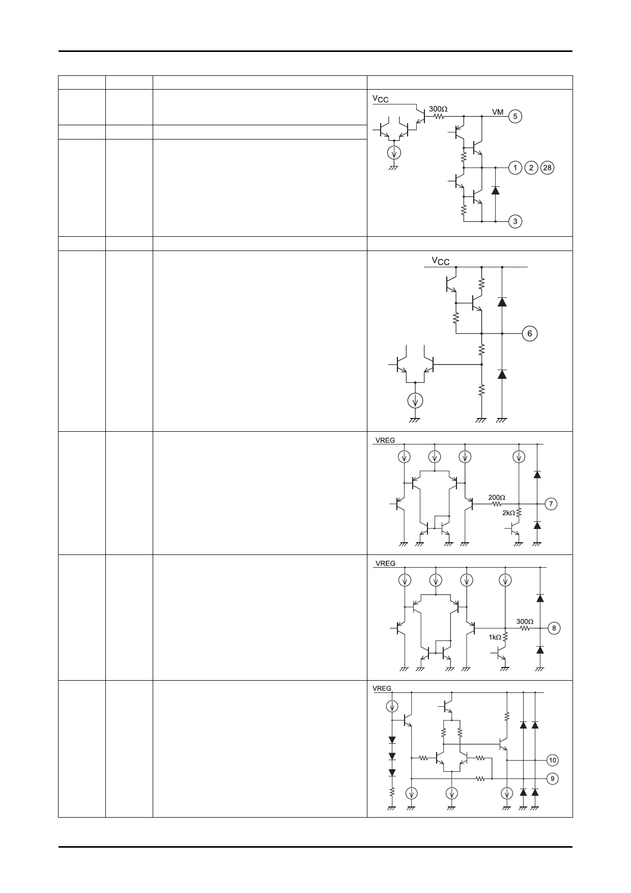
Pin Description
Pin No.
Pin name
Pin function
28
OUT1
1
OUT2
2
OUT3
3
GND2
Motor drive output pins.
Connect a Schottky diode between these outputs and VCC.
Output ground pin.
5
VM
Output block power supply and output current detection pin.
Connect a resistor (Rf) between this pin and VCC to detect the
output current as a voltage.
The output current is limited according to the equation IOUT =
VRF/Rf.
4
VCC
Power supply pin (except for output block).
6
VREG
Regulated power supply output pin (5V output).
Connect a capacitor (approx. 0.1μF) between this pin and
ground to stabilize the output.
Equivalent circuit
7
PWM
PWM frequency setting pin.
Connect a capacitor between this pin and ground.
C = 3900pF results in a frequency of about 18kHz.
8
CSD
Lock protection circuit operation time setting pin.
Connecting a capacitor of about 10μF between this pin and
ground results in a protection circuit operation time of about
3.3 seconds.
9
XI
10
XO
Crystal oscillator pins.
Connect to quartz oscillator to generate the reference clock.
When an external clock (of several MHz) is used, the clock
signal should be input via a resistor of about 5.1kΩ connected
in series with the XI pin. In this case, the XO pin must be left
open.
Continued on next page.
No.7099-6/11
Share Link: