LB1929 データシートの表示(PDF) - ON Semiconductor
部品番号
コンポーネント説明
メーカー
LB1929
ON Semiconductor

LB1929 Datasheet PDF : 11 Pages
| |||
LB1929
Continued from preceding page.
Pin No.
Pin name
Pin function
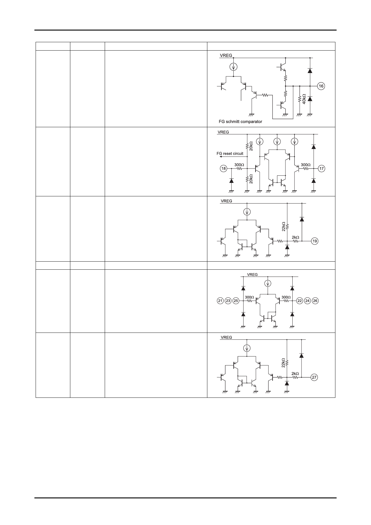
16
FGOUT
FG amplifier output pin.
Equivalent circuit
17
FGIN-
18
FGIN+
FG amplifier input pin.
By connecting a capacitor (approx. 0.1μF)
between FGIN+ and ground, the logic circuitry is
reset.
19
S/S
Start/stop control pin.
Start (Low) : 0V to 1.5V
Stop (High) : 3.5V to VREG
High when open.
Hysteresis width : approx. 0.5V.
20
GND1
22
IN1+
21
IN1-
24
IN2+
23
IN2-
26
IN3+
25
IN3-
Ground pin (except for output block).
Hall input pins.
High when IN+ > IN-, Low when IN+ < IN-.
Hall signal should have an amplitude of at least
100mVp-p (differential operation). When Hall
signal noise is a problem, connect a capacitor
between IN+ and IN-.
27
F/R
Forward/reverse control pin.
Forward (Low) : 0V to 1.5V
Reverse (High) : 3.5V to VREG
High when open.
Hysteresis width : approx. 0.5V.
No.7099-8/11
Share Link: