LB1929 データシートの表示(PDF) - ON Semiconductor
部品番号
コンポーネント説明
メーカー
LB1929
ON Semiconductor

LB1929 Datasheet PDF : 11 Pages
| |||
LB1929
Description of the LB1927
1. Speed control circuit
The IC performs speed control through combined use of a speed discrimination circuit and PLL circuit. The speed
control circuit counts FG cycles and outputs a deviation signal every 2FG cycles. The PLL circuit outputs a phase
deviation signal every FG cycle.
The FG servo frequency is determined by the following equation. The motor rotation speed is set by the number of
FG pulses and the crystal oscillator frequency.
fFG (servo) = fOSC/8192
fOSC : Crystal oscillator frequency
2. Output drive circuit
In order to reduce power loss at the output, the LB1929 uses the PWM drive technique. While ON, the output
transistors are always saturated, and motor drive power is adjusted by varying the output ON duty ratio. Because
output PWM switching is performed by the lower-side output transistor, a Schottky diode must be connected
between OUT and VCC. (If the reverse recovery time of the diode is too long, a feedthrough current will flow at the
instant when the lower-side transistor goes ON.) An internal diode is provided between OUT and GND. If large
output current causes a problem (waveform distortion during lower-side kickback, etc.), an external rectifying diode
or Schottky diode should be connected.
The output diode is integrated only on the lower side.
3. Current limiting circuit
The current limiting circuit limits the peak current to the value I = VRF/Rf (VRF = 0.5V typ., Rf : current detector
resistance). Current limiting is achieved by reducing the ON duty ratio of the output, which reduces the current.
4. Power save circuit
In order to reduce current drain in the STOP condition, the IC goes into power save mode. In this condition, bias
current to most circuits is cut off, but the 5V regulator output remains active.
5. Reference clock
The reference clock for speed control can be input using one of the following two methods.
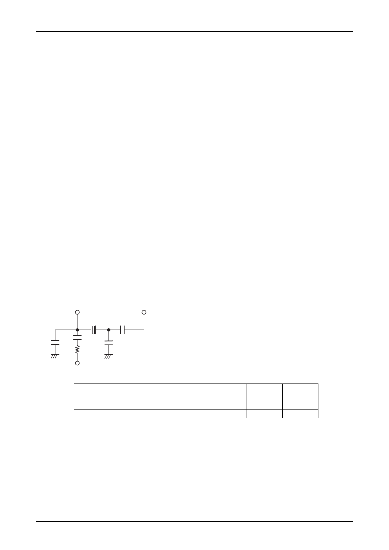
(1) Using a crystal oscillator
When a crystal is used for oscillation, connect the crystal, capacitors, and a resistor as shown in the figure below.
XI
XO
C1
C4
R1
C3
C2
C1, R1 : For stable oscillation
C3 : For oscillator coupling
C2 : For stabilization and to prevent oscillation at upper harmonic frequencies
C4 : Prevents oscillation at upper harmonic frequencies
VREG
Oscillator frequency (MHz)
3 to 5
5 to 8
8 to 10
C1 (μF)
0.1
0.1
0.1
C2 (pF)
15
10
10
C3 (pF)
47
47
22
(Reference values)
C4 (pF)
R1 (Ω)
10
330k
None
330k
None
330k
The circuit configuration and values are for reference only. The crystal oscillator’s characteristics as well as the
possibility of floating capacitance and noise due to layout factors must be taken into consideration when
designing an actual application.
No.7099-9/11
Share Link: