M54122L データシートの表示(PDF) - MITSUBISHI ELECTRIC
部品番号
コンポーネント説明
メーカー
M54122L Datasheet PDF : 6 Pages
| |||
MITSUBISHI <CONTROL / DRIVER IC>
M54122L
EARTH LEAKAGE CURRENT DETECTOR
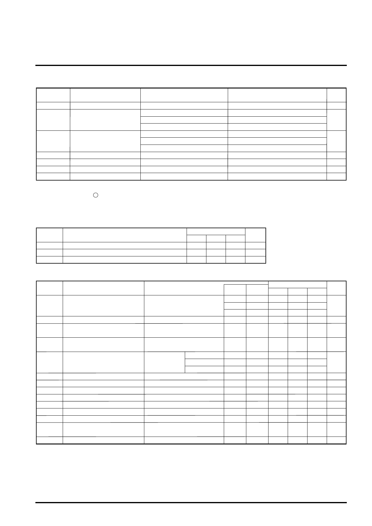
ABSOLUTE MAXIMUM RATINGS (Ta = -20 – 80°C unless otherwise noted)
Symbol
Parameter
Conditions
Ratings
Unit
IS
Supply current
Between VR-IN (Note 1)
IVR
VR terminal current
Between VR-GND
Between IN-VR (Note 1)
Between IN-VR (Note 1)
IIN
IN terminal current
Between IN-GND
Between VR-IN (Note 1)
ISC
SC terminal current
Pd
Power dissipation
Topr
Operating temperature
Tstg
Storage temperature
8
mA
250
30
mA
-250
250
30
mA
-250
5
mA
200
mW
-20 – 80
°C
-55 – 125
°C
Note 1: Current value between VR and IN, and between IN and VR is less than 1ms in the pulse width, and duty cycle is less than 12%. In applying AC current
continuously, it is 100mArms in the off-state.
Remarks: GND terminal (pin 3 ) of the circuit is a basis of all the voltages except differential input clamp voltage of DC electrical characteristics, and direction of
current is plus (no signal) in flowing into the circuit and is minus (– signal) in flowing out of it. Maximum value and minimum one are shown as
absolute value. Please don’t apply voltage whose standard is GND terminal in VR and IN pin.
RECOMMENDED OPERATING CONDITIONS (Ta = -20 – 80°C unless otherwise noted)
Symbol
VS
CVS
COS
Parameter
Supply voltage when latch circuit is off-state.
External capacitor between VS and GND
External capacitor between OS and GND
Limits
Unit
Min. Typ. Max.
12
V
1
µF
1
µF
ELECTRICAL CHARACTERISTICS (Ta = -20 – 80°C unless otherwise noted)
Symbol
Parameter
IS1
Supply current
VT
Trip voltage
ITD1
Timed current 1
Test conditions
VS = 12V, VR-VI = 30mV
VS = 16V, VR-VI (Note 2)
VS = 16V, VR-VI = 30mV
VOD = 1.2V
Tempera-
ture(°C)
-20
25
80
-20 – +80
Test
circuit
1
1
1
2
25
3
Limits
Min. Typ.∗ Max. Unit
580
400 530 µA
480
10 13.5 17 mVrms
-12
-30
µA
ITD2
Timed current 2
VS = 16V, short circuit between
VR and VI, VOD = 0.8V
25
4
17
37
µA
IO
Output current
VSC “ON”
ISC “ON”
IOSL
VIC
VIDC
VSM
IS2
SC ON voltage (Note 3)
SC input current
Output low-level current
Input clamp voltage
Differential input clamp voltage
Maximum current voltage
Supply current 2 (Note 4)
IS1 = 580µA
-20
5
VSC = 1.4V
VOS = 0.8V
IS1 = 530µA
25
5
IS1 = 480µA
80
5
VS = 16V
25
6
VS = 12V
25
7
VS = 12V, VOSL = 0.2V
-20 – +80
8
VS = 12V, IIC = 20mA
-20 – +80
9
IIDC = 100mA
-20 – +80 10
ISM = 7mA
25
11
VR-VI VOS = 0.6V (Note 5)
-20 – +80 12
-200
-100
-75
0.7
200
4.3
0.4
20
µA
1.4
V
5
µA
µA
6.7
V
2
V
28
V
900 µA
VS “OFF”
TON
Latch circuit off-state supply
voltage (Note 6)
Operating time (Note 7)
VS = 16V, VR-VI = 0.3V
25
13
0.5
25
14
2
V
4
ms
Note ∗: Typical values are at Ta = 25°C.
Note 2: When standard value of voltage (60Hz) between VR and VI is minimum, and output OS is low-level, or when standard value of voltage (60Hz) between
VR and VI is maximum, and output OS is high-level, it is considered as a good one.
Note 3: When standard value of voltage VSC “ON” is minimum, and output OS is low-level, or when standard value of voltage VSC “ON” is maximum, and output OS
is high-level, it is considered as a good one.
Note 4: Supply current 2 is necessary to keep high in output OS.
Note 5: After applying 30mV between VR and VI and shorting between them, it is considered as a good one if standard value of IGT flows out of output OS.
Note 6: After supply voltage applies 12V and output OS is high-level, it is considered as a good one in the standard value of supply voltage and in the low-level
of output OS.
Note 7: Operating time is a time from applying fixed input till operating latch circuit in 0.047µF between OD and GND.
Share Link: 