M54123L データシートの表示(PDF) - MITSUBISHI ELECTRIC
部品番号
コンポーネント説明
メーカー
M54123L Datasheet PDF : 6 Pages
| |||
MITSUBISHI <CONTROL / DRIVER IC>
M54123L
EARTH LEAKAGE CURRENT DETECTOR
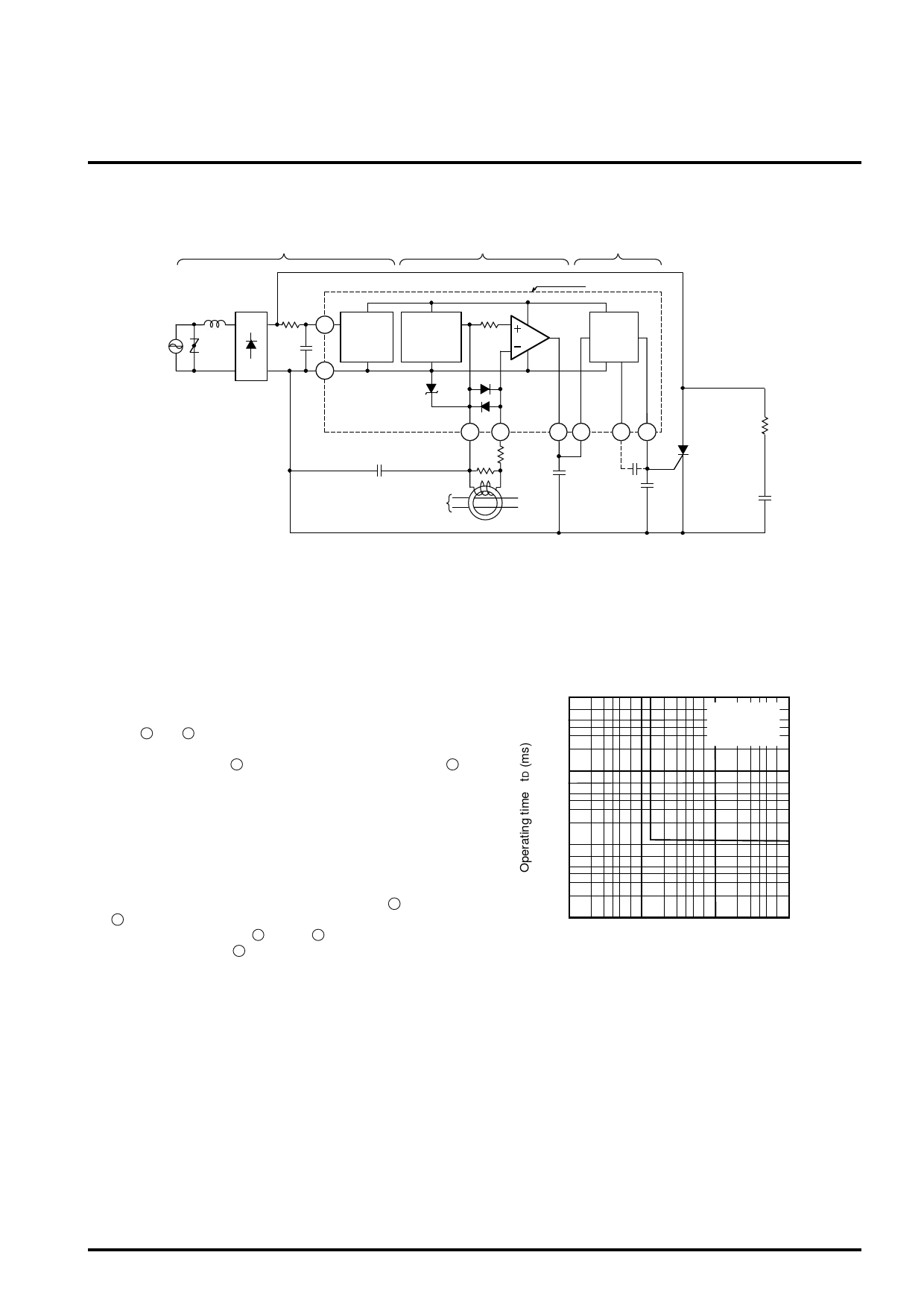
APPLICATION EXAMPLE
• HIGH-SPEED LEAKAGE CIRCUIT BREAKER WITH M54123L
Supply voltage circuit
Amplifier
Output circuit
Trip
coil
AC
line
R2 VS
8
C4
3
GND
Voltage
regulator
Reference
voltage
generator
M54123L
AMP
Latch
circuit
12
45
67
Note 8
R1
RP
RL 100Ω
SCR
C3
CR2AM
C1
CR03AM
C6
C2
CR02AM
AC
Note 9
C5
line
ZCT
Note 8 : Gate current must be selected.
Please select voltage resistance by AC supply voltage.
9 : MZ Core Series by Soryo Denshi Kagaku Co., Ltd (Mitsubishi Subsidiary)
Tel. +81-427-74-7813
Supply voltage circuit is connected as a previous diagram. Please
decide constants R1, R2, C4, and C5 of a filter in order to keep at
least 12V in VS, when normal supply current flows.
In this case, please connect C4 (more than 1µF) and C2 (less than
1µF). ZCT and load resistance RL of ZCT are connected between
input pin 1 and 2 . In this case protective resistance (RP = 100Ω)
must be insurted. Sensitivity current is regulated by RL, and output
of amplifier shows in pin 4 . External capacitor C1 between pin 44
and GND is used for noise removal.
When large current is grounded in the primary side (AC line) of
ZCT, the wave form in the secondary side of ZCT is distorted and
some signals doesn’t appear in the output of amplifier. So please
connect a varistor or a diode (2 pcs.) to ZCT in parallel.
Latch circuit is used to inspect the output level of amplifier and to
supply gate current on the external SCR. When input pin becomes
more than 1.1V (Typ.), latch circuit operates and supply gate
current in the gate of SCR connected to the output pin 7 .
Pin 6 can be used in the open state, but please connect capacitor
(about 0.047µF) between pin 6 and pin 7 .
Capacitor C6 between pin 1 and GND is used to remove noise and
is about 0.047µF.
1000
700
500
300
Operating time vs. input voltage
C1 = 0.047µF
Ta = 25°C
60HZ
100
70
50
30
10
7
5
3
1
1
3 5 7 10 30 50 100 300 1000
70
500
Input voltage V1 (mVrms)
Share Link: 