M63015FP データシートの表示(PDF) - MITSUBISHI ELECTRIC
部品番号
コンポーネント説明
メーカー
M63015FP Datasheet PDF : 15 Pages
| |||
MITSUBISHI SEMICONDUCTOR (LSI)
M63015FP
SPINDLE MOTOR AND 4CH ACTUATOR DRIVER
q PWM carrier frequency setting
PWM carrier frequency is decided by charging and discharging the
capacitor that is connected to OSC terminal outer IC. Examination
of the relationship the capacitor connected to OSC terminal and
PWM carrier frequency is given in following table.
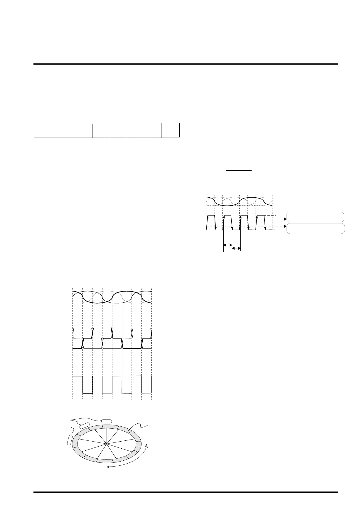
q FG function duty at spindle drive
The FG terminal outputs the square pulse signal synchronizing
with the hall inputs (Hu+,Hu-,Hv+, Hv-,Hw+,Hw-) timing. and, the
FG terminal is open-collector output. (cf. FG timing chart on the
previous page)
Capacitor [pF]
330
Carrier Frequency [kHz] 65
220 180
90 110
130 110
140 160
Note : This PWM carrier frequency is typ value.
q FG function duty at spindle drive
FG function DUTY is shown in a below equation at rihgt Figure.
q Recommendation of short brake mode at spindle drive
This IC has two brake mode, PWM-BRAKE-MODE and SHORT-
BRAKE-MODE. In this IC recommendation, SHORT-BRAKE-
Ton
FG DUTY [%] =
Ton + Toff
MODE is superior to PWM-BRAKE-MODE to reducing the power
dissipation and to avoid breaking down of this IC.
Hw+ Hv+ Hu+
(By excessive reverse torque current in braking a motor with
Hall
input
PWM-BRAKE from high-speed-rotation with being excessive Back-
EMF, this IC could be broken.)
q The relationship between hall-amplifier-input and
output-current-commutation/FG output at spindle
drive
FG
output
Ton
Toff
FG pull-up R:10kΩ
FG output voltage:5V
FG output frequency:3kHz
(SPM motor rev 10000rpm)
Hall input signal level : 80mVp-p
5V
FG High voltage threshold:3.2V
FG Low voltage threshold:0.8V
0V
The relationship between the hall elements, the motor output
current and FG output(18pulse/rotation)
are shown in bellow Figure.
Hall
input
Hw+
Hv+
Hu+
q Phase delay circuit at slide
Phase delay circuit is built in the IC to detect an output spike
current, when the motor current direction is switching.
In switching the motor current direction, Phase delay circuit switch-
off all output trangister of H-bridge for 3µsec.
V
U
W
V
+
Output
current 0
-
UW
V
U
W
q Output current setting at slide
In this IC, since output tranjister is NPN-type tranjister, motor coil
current (Io) is larger than sensing resistance current about 20mA
(TYP.) according to base current of output tranjister.
Therefore please design output current with consisting these base
current.
FG
output
Hall elements
UW
V
V
W
U
U
V
W
Forward
SPIN > REF
Outer roter
Reverse
SPIN < REF
Share Link: 