QL8150-8PS484C(2002) データシートの表示(PDF) - QuickLogic Corporation
部品番号
コンポーネント説明
メーカー
QL8150-8PS484C
(Rev.:2002)
(Rev.:2002)
QuickLogic Corporation

QL8150-8PS484C Datasheet PDF : 49 Pages
| |||
(FOLSVH,, )DPLO\ 'DWD 6KHHW 5HY %
,2 &HOO 6WUXFWXUH
Eclipse-II features a variety of distinct I/O pins to maximize performance, functionality, and
flexibility with bi-directional I/O pins and input-only pins. All input and I/O pins are 1.8 V, 2.5 V,
and 3.3 V tolerant and comply with the specific I/O standard selected. For single ended I/O
standards, VCCIO specifies the input tolerance and the output drive. For voltage referenced I/O
standards (e.g SSTL), the voltage supplied to the INREF pins in each bank specifies the input
switch point. For example, the VCCIO pins must be tied to a 3.3 V supply to provide 3.3 V
compliance. Eclipse-II can also support the LVDS and LVPECL I/O standards with the use of
external resistors ( see 7DEOH ).
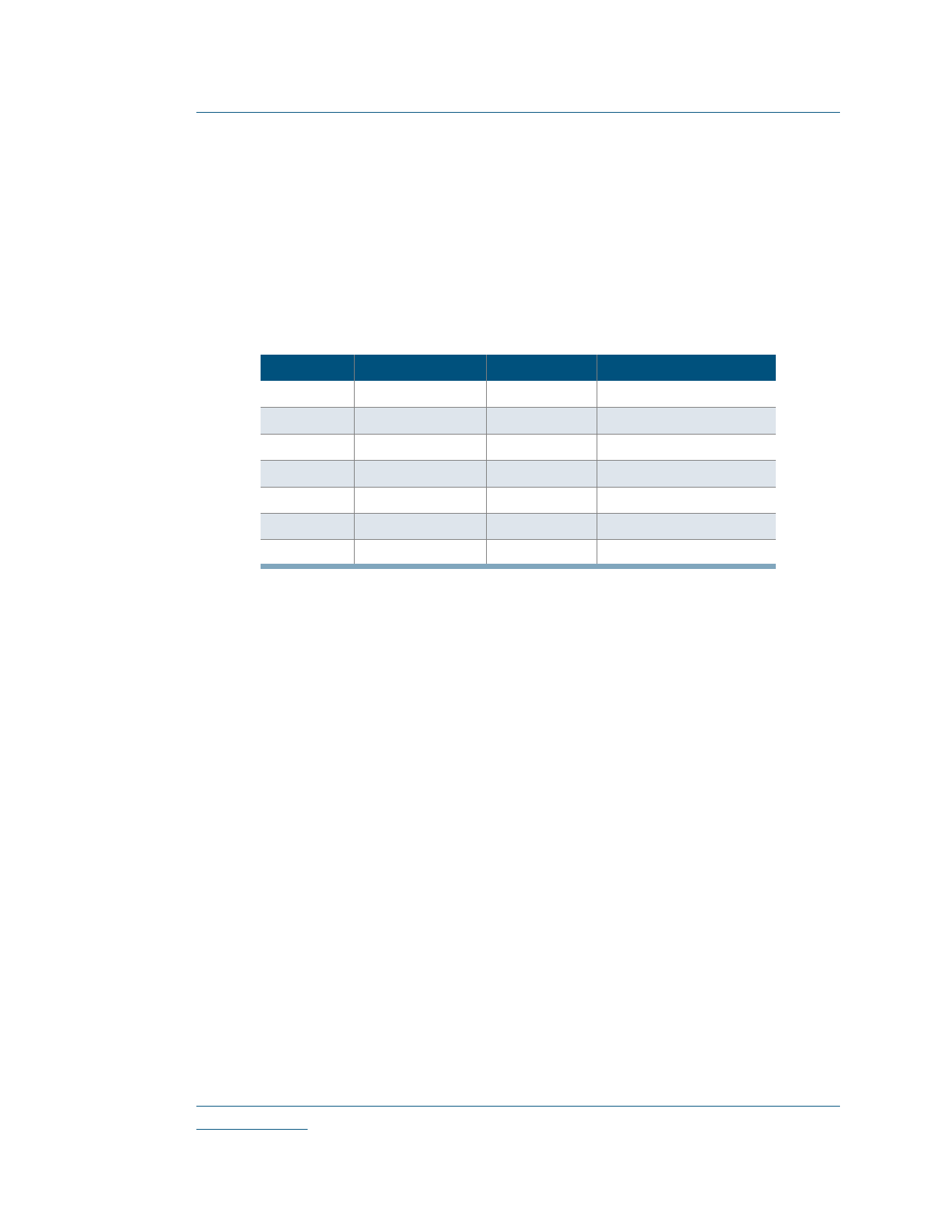
7DEOH
,2 6WDQGDUGV DQG $SSOLFDWLRQV
,2 6WDQGDUG 5HIHUHQFH 9ROWDJH 2XWSXW 9ROWDJH
$SSOLFDWLRQ
LVTTL
n/a
3.3 V
General Purpose
LVCMOS25
n/a
2.5 V
General Purpose
LVCMOS18
n/a
1.8 V
General Purpose
PCI
n/a
3.3 V
PCI Bus Applications
GTL+
1
n/a
Backplane
SSTL3
1.5
3.3 V
SDRAM
SSTL2
1.25
2.5 V
SDRAM
As designs become more complex and requirements more stringent, several
application-specific I/O standards have emerged for specific applications. I/O standards for
processors, memories, and a variety of bus applications have become commonplace and a
requirement for many systems. In addition, I/O timing has become a greater issue with specific
requirements for setup, hold, clock to out, and switching times. Eclipse-II has addressed these new
system requirements and now includes a completely new I/O cell which consists of programmable
I/Os as well as a new cell structure consisting of three registers—Input, Output, and OE.
Eclipse-II offers banks of programmable I/Os that address many of the bus standards that are
popular today. As shown in )LJXUH each bi-directional I/O pin is associated with an I/O cell
which features an input register, an input buffer, an output register, a three-state output buffer, an
output enable register, and 2 two-to-one output multiplexers.
ZZZTXLFNORJLFFRP
Preliminary 4XLFN/RJLF &RUSRUDWLRQ
Share Link: