QL8150-8PS484C(2002) データシートの表示(PDF) - QuickLogic Corporation
部品番号
コンポーネント説明
メーカー
QL8150-8PS484C
(Rev.:2002)
(Rev.:2002)
QuickLogic Corporation

QL8150-8PS484C Datasheet PDF : 49 Pages
| |||
(FOLSVH,, )DPLO\ 'DWD 6KHHW 5HY %
NOTE: +) VWDQGV IRU KLJK IUHTXHQF\ DQG /) VWDQGV IRU ORZ IUHTXHQF\
3// 0RGHO
PLL_HF
PLL_LF
PLL_MULT2HF
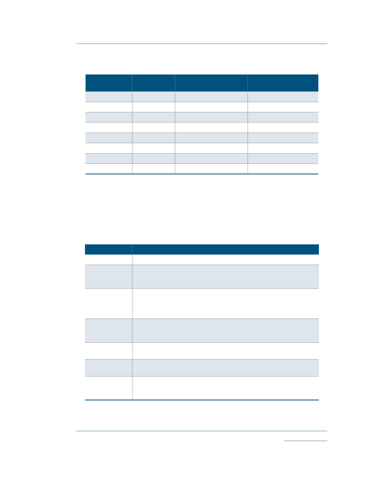
7DEOH
3// 0RGH )UHTXHQFLHV
2XWSXW
)UHTXHQF\
,QSXW )UHTXHQF\ 5DQJH
Same as input
66 MHz–150 MHz
Same as input
25 MHz–133 MHz
2x
50 MHz–125 MHz
2XWSXW )UHTXHQF\ 5DQJH
66 MHz–150 MHz
25 MHz–133 MHz
100 MHz–250 MHz
PLL_MULT2LF
2x
16 MHz–50 MHz
32 MHz–100 MHz
PLL_DIV2HF
1/2x
100 MHz–250 MHz
50 MHz–125 MHz
PLL_DIV2LF
PLL_MULT4
1/2x
4x
50 MHz–100 MHz
16 MHz–40 MHz
25 MHz–50 MHz
64 MHz–160 MHz
PLL_DIV4
1/4x
100 MHz–300 MHz
25 MHz–75 MHz
The input frequency can range from 16 MHz to 300 MHz, while output frequency ranges from
25 MHz to 250 MHz. When you add PLLs to your top-level design, be sure that the PLL mode
matches your desired input and output frequencies.
3// 6LJQDOV
7DEOH summarizes the key signals in QuickLogic's PLLs.
7DEOH
4XLFN/RJLF 3// 6LJQDOV
6LJQDO 1DPH
'HVFULSWLRQ
PLLCLK_IN Input clock signal
PLL_RESET
Active High Reset If PLL_RESET is asserted, then CLKNET_OUT and
PLLPAD_OUT are reset to 0. This signal must be asserted and then released
in order for the LOCK_DETECT to work.
ONn_OFFCHIP
PLL output This signal selects whether the PLL will drive the internal clock
network or be used off-chip. This is a static signal, not a dynamic signal.
Tied to GND = outgoing signal drives internal gates.
Tied to VCC = outgoing signal used off-chip.
Out to internal gates This signal bypasses the PLL logic before driving the
CLKNET_OUT internal gates. Note that this signal cannot be used in the same quadrant where
the PLL signal is used (PLLCLK_OUT).
PLLCLK_OUT
Out from PLL to internal gates This signal can drive the internal gates after
going through the PLL. For this to work, ONn_OFFCHIP must be tied to GND.
PLLPAD_OUT
Out to off-chip This outgoing signal is used off-chip. For this to work,
ONn_OFFCHIP signal must be tied to VCC.
Active High Lock detection signal NOTE: For simulation purposes, this
LOCK_DETECT signal gets asserted after 10 clock cycles. However, it can take a maximum of
200 clock cycles to sync with the input clock upon release of the RESET signal.
NOTE: %HFDXVH 3//&/.B,1 DQG 3//B5(6(7 VLJQDOV KDYH3//B,13$' DQG 3//3$'B287
KDV 2873$' \RX GR QRW KDYH WR DGG DGGLWLRQDO SDGV WR \RXU GHVLJQ
Preliminary 4XLFN/RJLF &RUSRUDWLRQ
ZZZTXLFNORJLFFRP
Share Link: