BF998WR データシートの表示(PDF) - Philips Electronics
部品番号
コンポーネント説明
メーカー
BF998WR Datasheet PDF : 12 Pages
| |||
Philips Semiconductors
N-channel dual-gate MOS-FET
Product specification
BF998WR
VDD
140
kΩ
VAGC
1 nF
50 Ω
input
,,,,270
100 kΩ 1 nF
kΩ
L1
1 nF
1 nF
L2
C1
2-18 pF
C2
0.5-3.5 pF
VDD
1 nF
,, 1 nF
L4
L3
C3
0.5-3.5 pF
1 nF
50 Ω
input
C4
4-40 pF
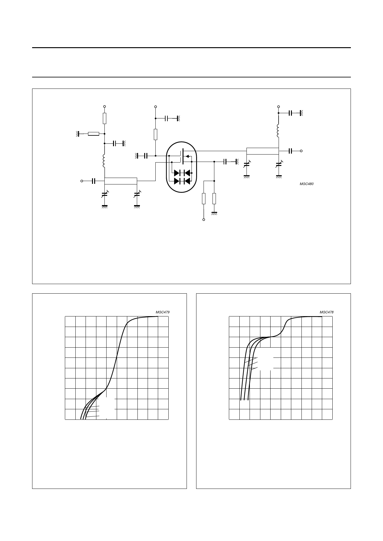
MGC480
1.8
360
kΩ
Ω
VDD
VDD = 12 V; GS = 3.3 mS; GL = 1 mS.
L1 = L4 = 200 nH; 11 turns 0.5 mm copper wire, without spacing, internal diameter 3 mm.
L2 = 2 cm, silvered 0.8 mm copper wire, 4 mm above ground plane.
L3 = 2 cm, silvered 0.5 mm copper wire, 4 mm above ground plane.
Fig.16 Gain control test circuit at f = 800 MHz.
0
∆Gtr
(dB)
−10
MGC479
−20
−30
−40
−50
0
IDSS=
max
typ
min
2
4
6
8
10
VAGC(V)
0
∆Gtr
(dB)
−10
−20
−30
IDSS=
max
typ
min
MGC478
−40
−50
0
2
4
6
8
10
VAGC(V)
VDD = 12 V; f = 200 MHz; Tamb = 25 °C.
Fig.17 Automatic gain control characteristics
measured in circuit of Fig.15.
1997 Sep 05
VDD = 12 V; f = 800 MHz; Tamb = 25 °C.
Fig.18 Automatic gain control characteristics
measured in circuit of Fig.16.
9
Share Link: 