ATA6613C データシートの表示(PDF) - Atmel Corporation
部品番号
コンポーネント説明
メーカー
ATA6613C
Atmel Corporation

ATA6613C Datasheet PDF : 312 Pages
| |||
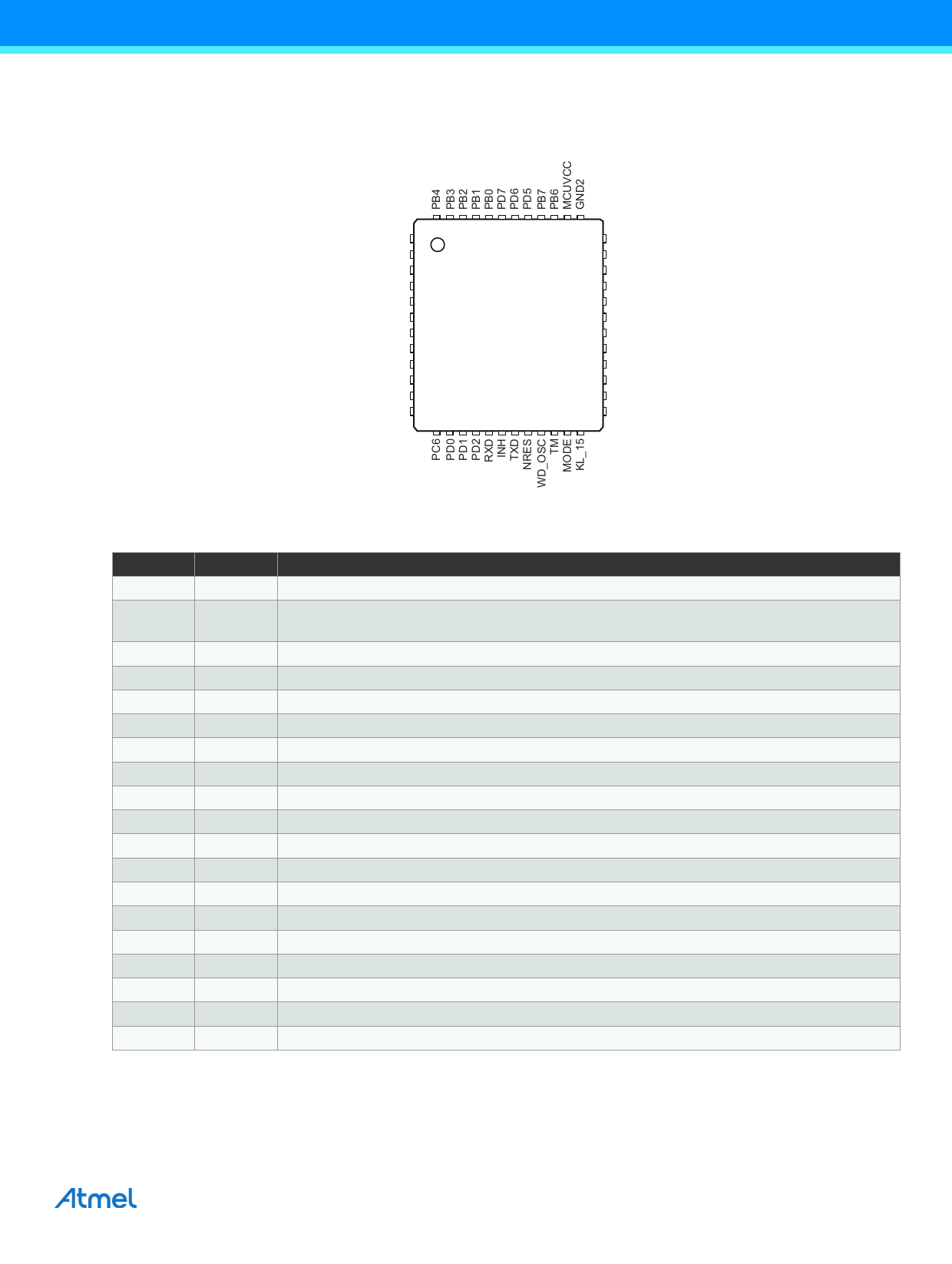
1. Pin Configuration
Figure 1-1. Pinning QFN48, 7mm × 7mm
PB5
MCUAVCC
ADC6
AREF
GND4
ADC7
PC0
PC1
PC2
PC3
PC4
PC5
48 47 46 45 44 43 42 41 40 39 38 37
1
36
2
35
3
34
4
33
5
Atmel
32
6
ATA6612C/ 31
7
ATA6613C 30
8
29
9
28
10
27
11
26
12
25
13 14 15 16 17 18 19 20 21 22 23 24
MCUVCC
GND1
PD4
PD3
LIN
GND
WAKE
NTRIG
EN
VS
VCC
PVCC
Table 1-1. Pin Description
Pin
1
2
3
4
5
6
7
8
9
10
11
12
13
14
15
16
17(1)
18(1)
19(1)
Note: 1.
Symbol Function
PB5 Port B 5 I/O line (SCK / PCINT5)
MCUAVCC
Microcontroller ADC-unit supply voltage (referred to as AVCC pin in Section 5. “Microcontroller
Block” on page 27 and Section 6. “2-wire Serial Interface Characteristics” on page 276)
ADC6 ADC input channel 6
AREF Analog reference voltage input
GND4 Ground
ADC7 ADC input channel 7
PC0 Port C 0 I/O line (ADC0/PCINT8)
PC1 Port C 1 I/O line (ADC1/PCINT9)
PC2 Port C 2 I/O line (ADC2/PCINT10)
PC3 Port C 3 I/O line (ADC3/PCINT11)
PC4 Port C 4 I/O line (ADC4/SDA/PCINT12)
PC5 Port C 5 I/O line (ADC5/SCL/PCINT13)
PC6 Port C 6 I/O line (RESET/PCINT14)
PD0 Port D 0 I/O line (RXD/PCINT16)
PD1 Port D 1 I/O line (TXD/PCINT17)
PD2 Port D 2 I/O line (INT0/PCINT18)
RXD Receive data output
INH High side switch output for controlling an external voltage regulator
TXD Transmit data input / active low output after a local wake up request
This identifies the pins of the LIN SBC Atmel ATA6624
ATA6612C/ATA6613C [DATASHEET]
3
9111L–AUTO–11/14
Share Link: