MC145406P データシートの表示(PDF) - LANSDALE Semiconductor Inc.
部品番号
コンポーネント説明
メーカー
MC145406P Datasheet PDF : 10 Pages
| |||
ML145406
LANSDALE Semiconductor, Inc.
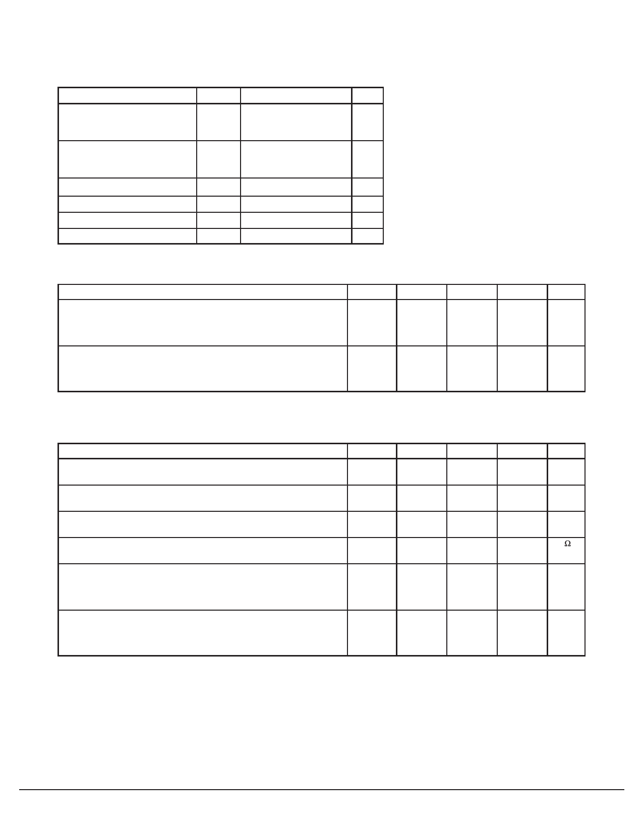
MAXIMUM RATINGS (Voltage polarities referenced to GND)
Rating
Symbol
Value
Unit
DC Supply Voltages (VDD ≥ VCC)
Input Voltage Range
Rx1–3 Inputs
DI1–3 Inputs
DC Current Per Pin
VDD
VSS
VCC
VIR
– 0.5 to + 13.5
V
+ 0.5 to – 13.5
– 0.5 to + 6.0
V
(VSS – 15) to (VDD + 15)
– 0.5 to (VCC + 0.5)
± 100
mA
Power Dissipation
PD
Operating Temperature Range
TA
Storage Temperature Rate
Tstg
1.0
W
– 40 to + 85
°C
– 85 to + 150
°C
This device contains protection circuitry to pro-
tect the inputs against damage due to high static
voltages or electric fields; however, it is advised
that normal precautions be taken to avoid applica-
tion of any voltage higher than maximum rated
voltages to this high impedance circuit. For proper
operation, it is recommended that the voltages at
the DI and DO pins be constrained to the range
GND ≤VDI≤ VCC and GND≤ VDO ≤ VCC. Also, the
voltage at the Rx pin should be constrained to
(VSS – 15 V) ≤ VRx1–3 ≤ (VDD + 15 V), and Tx
should be constrained to VSS ≤ VTx1–3 ≤ VDD.
Unused inputs must always be tied to an ap-
propriate logic voltage level (e.g., GND or VCC for
DI and Ground for Rx.)
DC ELECTRICAL CHARACTERISTICS (All polarities referenced to GND = 0 V, TA = – 40 to + 85°C)
Parameter
Symbol
Min
Typ
Max
Unit
DC Supply Voltage
VDD
VSS
VCC (VDD ≥ VCC)
Quiescent Supply Current (Outputs unloaded, inputs low)
VDD = + 12 V
VSS = – 12 V
VCC = + 5 V
VDD
VSS
VCC
IDD
ISS
ICC
V
4.5
5 to 12
13.2
– 4.5 – 5 to – 12 – 13.2
4.5
5.0
5.5
µA
—
140
400
—
340
600
—
300
450
RECEIVER ELECTRICAL SPECIFICATIONS
(Voltage polarities referenced to GND = 0 V, VDD = + 5 to + 12 V, VSS = – 5 to – 12 V, VDD ≥ VCC, TA = – 40 to + 85°C)
Characteristic
Symbol
Min
Typ
Max
Unit
Input Turn–on Threshold
VDO1–DO3 = VOL, VCC = 5.0 V ± 5%
Rx1–Rx3
Von
1.35
1.80
2.35
V
Input Turn–off Threshold
VDO1–DO3 = VOH, VCC = 5.0 V ± 5%
Rx1–Rx3
Voff
0.75
1.00
1.25
V
Input Threshold Hysteresis
VCC = 5.0 V ± 5%
Rx1–Rx3 Von–Voff
0.6
0.8
—
V
Input Resistance
(VSS – 15 V) ≤ VRx1–Rx3 ≤ (VDD + 15 V)
Rx1–Rx3
Rin
3.0
5.4
7.0
k
High–Level Output Voltage (VRx1–Rx3 = – 3 V to (VSS – 15 V))*
VOH
DO1–DO3
4.9
4.9
IOH = – 20 µA, VCC = + 5.0 V
IOH = – 1 mA, VCC = + 5.0 V
3.8
4.3
V
—
—
Low–Level Output Voltage (VRx1–Rx3 = + 3 V to (VDD + 15 V))* DO1–DO3 VOL
V
IOL = + 20 µA, VCC = + 5.0 V
—
0.01
0.1
IOL = + 2 mA, VCC = + 5.0 V
—
0.02
0.5
IOL = + 4 mA, VCC = + 5.0 V
—
0.5
0.7
* This is the range of input voltages as specified by EIA 232–E to cause a receiver to be in the high or low logic state.
Page 2 of 10
www.lansdale.com
Issue A
Share Link: 