FM24CL64B-GA データシートの表示(PDF) - Cypress Semiconductor
部品番号
コンポーネント説明
メーカー
FM24CL64B-GA Datasheet PDF : 13 Pages
| |||
To perform a selective read, the bus master sends out
the slave address with the LSB set to 0. This specifies
a write operation. According to the write protocol,
the bus master then sends the address bytes that are
loaded into the internal address latch. After the
FM24CL64B - Automotive Temp.
FM24CL64B acknowledges the address, the bus
master issues a start condition. This simultaneously
aborts the write operation and allows the read
command to be issued with the slave address LSB set
to a „1‟. The operation is now a current address read.
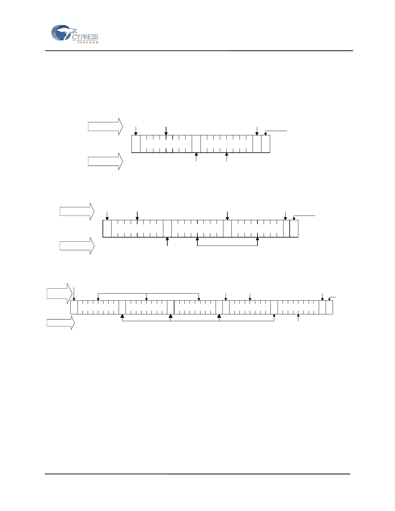
By Master
Start
Address
S
Slave Address 1 A
No
Acknowledge
Data Byte
1P
Stop
By F-RAM
Acknowledge Data
Figure 7. Current Address Read
By Master
Start
Address
S
Slave Address 1 A
Acknowledge
No
Acknowledge
Data Byte
A
Data Byte
1P
Stop
By F-RAM
Acknowledge
Data
Figure 8. Sequential Read
Start
By Master
S
Slave Address 0 A
Address
Address MSB
A
Address LSB
Start
Address
AS
Slave Address 1 A
By F-RAM
Acknowledge
Figure 9. Selective (Random) Read
No
Acknowledge
Stop
Data Byte
1P
Data
Document Number: 001-84457 Rev. *A
Page 7 of 13
Share Link: 