TSA5059TS データシートの表示(PDF) - Philips Electronics
部品番号
コンポーネント説明
メーカー
TSA5059TS Datasheet PDF : 24 Pages
| |||
Philips Semiconductors
2.7 GHz I2C-bus controlled low phase
noise frequency synthesizer
Preliminary specification
TSA5059
XT/COMP frequency output
It is possible to output either the crystal or the comparison
frequency at this pin to be used in the application, for
example to drive a second PLL synthesizer, saving a
quartz crystal in the bill of material. To output fxtal, it is
necessary to set bit XCE to logic 1 and bit XCS to logic 0,
or bit XCE to logic 0 and bit XCS to logic 1 during a test
mode, while to output fcomp, it is necessary to set both
bits XCE and XCS to logic 1.
If the output signal at this pin is not used, it is
recommended to disable it, setting both bits XCE and XCS
to logic 0. Table 10 shows how this pin is programmed.
At power-on, the XT/COMP output is set, with the fxtal
signal selected.
Prescaler enable
Even if the TSA5059 is able to work with the relation
fcomp = step size for an input frequency up to 2.7 GHz, this
IC is designed to be backward compatible with existing ICs
for which this relation is only valid for an RF frequency up
to 2.0 GHz and in which it is necessary to select a fixed
divide-by-two prescaler for frequencies between 2.0 and
2.7 GHz.
The prescaler is selected by setting bit PE to logic 1 and
it is not in use if bit PE is set to logic 0.
For new designs, and especially if it is important to reach
a low phase noise on the controlled VCO, it is
recommended to set bit PE to logic 0, and not to use the
prescaler, allowing the comparison frequency to be equal
to the step size, whatever the RF frequency is between
64 and 2700 MHz.
Test modes
It is possible to access the test modes setting bit XCE to
logic 0 and bit XCS to logic 1. One specific test mode is
then selected using bits T2, T1 and T0, as described in
Table 10.
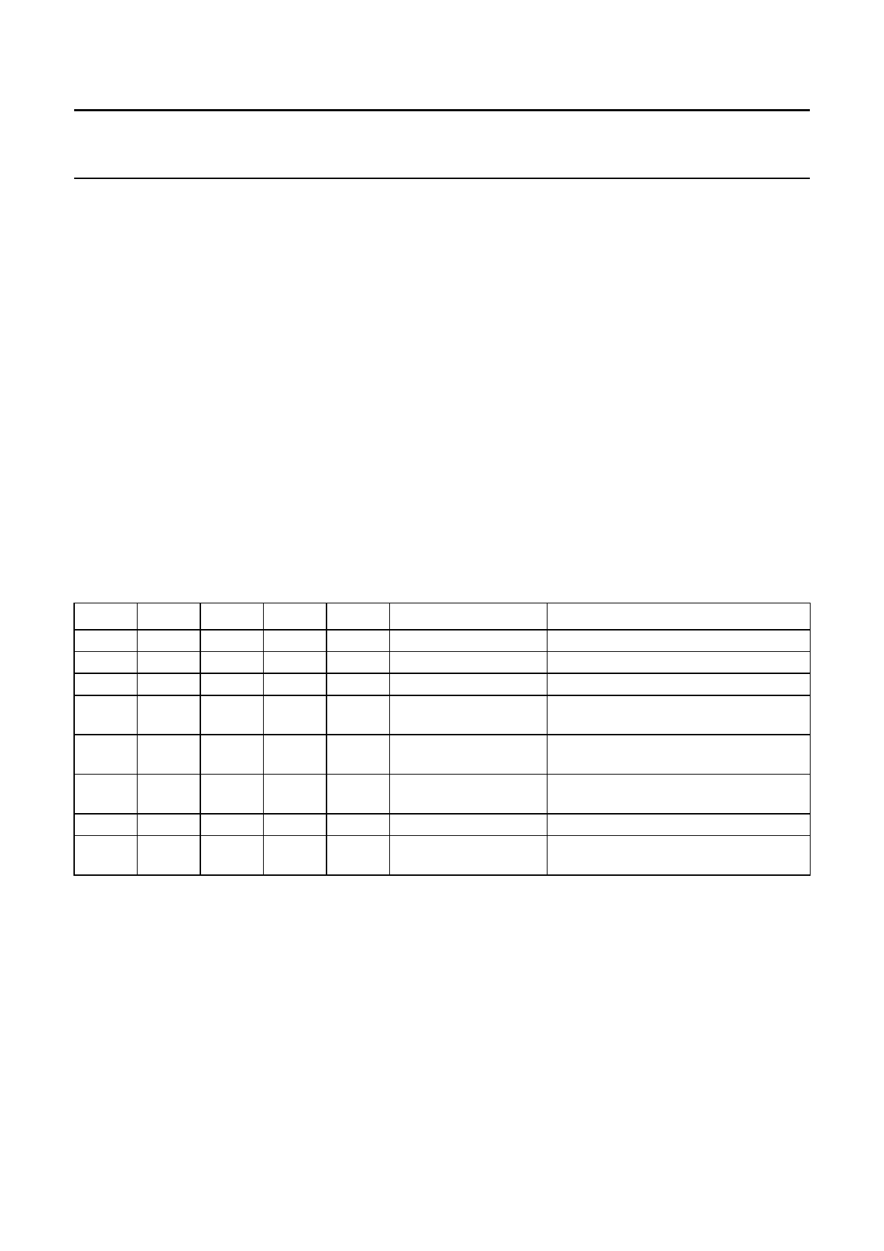
Table 10 XT/COMP and test mode selection; note 1
XCE XCS
T2
T1
T0
XT/COMP OUTPUT
TEST MODE
0
0
X
X
X disabled
normal operation
1
0
X
X
X
fxtal
1
1
X
X
X
fcomp
0
1
0
0
0
fxtal
normal operation
normal operation
test operation: charge pump sink;
status byte: bit FL = 1
0
1
0
0
1
fxtal
test operation: charge pump source;
status byte: bit FL = 0
0
1
0
1
0
fxtal
0
1
0
1
1
fxtal
0
1
1
X
X
fxtal
test operation: charge pump disabled;
status byte: bit FL = 0
test operation: 1⁄2fDIV switched to Port P0
test operation: tuning voltage (pin VT) is
off (high-impedance); note 2
Notes
1. X = don’t care.
2. Status at Power-on reset.
1999 Oct 05
10
Share Link: 