MGF7169C データシートの表示(PDF) - MITSUBISHI ELECTRIC
部品番号
コンポーネント説明
メーカー
MGF7169C Datasheet PDF : 20 Pages
| |||
Preliminary
information
MITSUBISHI SEMICONDUCTOR <GaAs MMIC>
MGF7169C
UHF BAND GaAs POWER AMPLIFIER
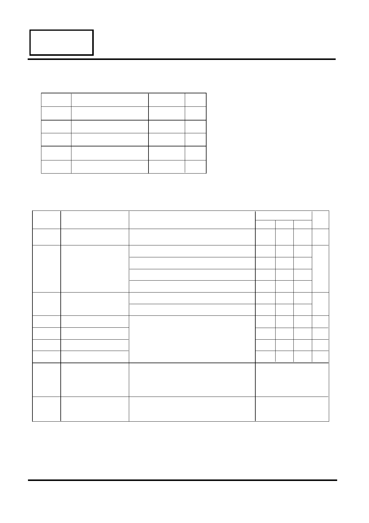
ABSOLUTE MAXIMUM RATINGS (Ta=25˚C)
Symbol
Parameter
Ratings Unit
Vd1,Vd2 Drain supply voltage
6
V
Vg
Gate supply voltage
-4
V
Pi
Input power
15
dBm
Tc(op) Operating case temperature -30 ~ +85 ˚C
Tstg
Storage temperature
-30 ~ +100 ˚C
*1.Each maximum rating is guaranteed independently.
ELECTRICAL CHARACTERISTICS (Ta=25˚C)
Symbol
Parameter
Test conditions
Limits
Unit
MIN TYP MAX
f
frequency
1850 — 1910 MHz
ACP<-42dBc (1.25MHz off-set.) Vd1=Vd2=3.0V
— 450 —
Idt
Total drain current
Idle_Id Idle current
Pout
Ig
2sp
rin
Output power
Gate current
2nd harmonics
input VSWR
ACP<-44dBc (1.25MHz off-set.) Vd1=Vd2=3.0V
ACP<-46dBc (1.25MHz off-set.) Vd1=Vd2=3.0V
ACP<-44dBc (1.25MHz off-set.) Vd1=Vd2=3.3V
Vg1=Vg2=-2.0V, Po=28dBm
Vg1=Vg2=-2.5V, Po=12dBm
Vd1=Vd2=3.0V,Vg1=Vg2=-2.0V,
Pin=7dBm CDMA modulated signal
based on IS-95 STD.
(1.2288Mbps spreading,OQPSK)
— 480 —
mA
— 520 —
— 450 —
— 150 —
mA
— 50 —
— 28 — dBm
— — -3 mA
— — -30 dBc
—— 3—
Vd1=Vd2=3.0V,
—
Damage
with-standing
Pin=7dBm,
Load VSWR=10, All phase
Note Time=10 sec
No damage
Vd1=Vd2=3.0V,
—
Stability
Pin=7dBm,
Note Load VSWR=3:1, All phase
No oscillation
Spurious level≤-60dBc
*CDMA is code division multiple Access. OQPSK is modulation method, off-set quadrature phase shift keying.
Electrical characteristics are changed by the external matching circuit.
Limits are guaranteed by using MITSUBISHI test fixture.
Note : Sampling inspection
MITSUBISHI ELECTRIC
(2/20)
Aug. '97
Share Link: 