SDS120 データシートの表示(PDF) - XP Power Limited
部品番号
コンポーネント説明
メーカー
SDS120 Datasheet PDF : 2 Pages
| |||
Models and Ratings
SDS120
Max.
Power
72.0 W
110.0 W
115.0 W
120.0 W
120.0 W
120.0 W
120.0 W
120.0 W
120.0 W
120.0 W
120.0 W
120.0 W
120.0 W
120.0 W
120.0 W
79.5 W
120.0 W
120.0 W
91.5 W
91.5 W
120.0 W
120.0 W
120.0 W
120.0 W
120.0 W
120.0 W
120.0 W
120.0 W
120.0 W
120.0 W
120.0 W
120.0 W
120.0 W
120.0 W
120.0 W
120.0 W
Vnom
3.3 V
5.0 V
7.0 V
9.0 V
12.0 V
15.0 V
18.0 V
24.0 V
28.0 V
36.0 V
48.0 V
3.3 V
5.0 V
5.0 V
5.0 V
3.3 V
5.0 V
28.0 V
3.3 V
3.3 V
3.3 V
3.3 V
3.3 V
3.3 V
5.0 V
5.0 V
5.0 V
5.0 V
5.0 V
5.0 V
5.0 V
5.0 V
5.0 V
5.0 V
5.0 V
5.0 V
Output 1
Imin
Imax
0.00 A 22.00 A
0.00 A 22.00 A
0.00 A 16.42 A
0.00 A 13.33 A
0.00 A 10.00 A
0.00 A 8.00 A
0.00 A 6.66 A
0.00 A 5.00 A
0.00 A 4.28 A
0.00 A 3.33 A
0.00 A 2.50 A
1.50 A 15.00 A
1.50 A 15.00 A
1.50 A 15.00 A
1.50 A 15.00 A
1.50 A 15.00 A
1.50 A 15.00 A
0.39 A 3.92 A
1.50 A 15.00 A
1.50 A 15.00 A
1.50 A 15.00 A
1.50 A 15.00 A
1.50 A 15.00 A
1.50 A 15.00 A
1.50 A 15.00 A
1.50 A 15.00 A
1.50 A 15.00 A
1.50 A 15.00 A
1.50 A 15.00 A
1.50 A 15.00 A
1.50 A 15.00 A
1.50 A 15.00 A
1.50 A 15.00 A
1.50 A 15.00 A
1.50 A 15.00 A
1.50 A 15.00 A
Tol.(1)
5%
5%
5%
4%
3%
3%
3%
2%
2%
2%
2%
5%
5%
5%
5%
5%
5%
5%
5%
5%
5%
5%
5%
5%
5%
5%
5%
5%
5%
5%
5%
5%
5%
5%
5%
5%
Vnom
Output 2
Imin
Imax
12.0 V
12.0 V
15.0 V
24.0 V
5.0 V
-24.0 V
5.0 V
5.0 V
5.0 V
12.0 V
12.0 V
12.0 V
12.0 V
12.0 V
12.0 V
12.0 V
12.0 V
15.0 V
15.0 V
24.0 V
24.0 V
24.0 V
24.0 V
10.0 V
10.0 V
0.20 A
0.20 A
0.20 A
0.10 A
0.40 A
0.20 A
0.20 A
0.60 A
0.60 A
0.60 A
0.60 A
0.60 A
0.60 A
0.60 A
0.60 A
0.60 A
0.60 A
0.60 A
0.60 A
0.35 A
0.35 A
0.35 A
0.35 A
0.60 A
0.60 A
6.0 A
6.0 A
6.0 A
3.5 A
6.0 A
2.0 A
2.0 A
6.0 A
6.0 A
6.0 A
6.0 A
6.0 A
6.0 A
6.0 A
6.0 A
6.0 A
6.0 A
6.0 A
6.0 A
3.5 A
3.5 A
3.5 A
3.5 A
6.0 A
6.0 A
Tol.(1)
Vnom
Output 3
Imin
Imax
5%
5%
5%
5%
5%
5%
5%
5%
12.0 V 0.00 A 1.0 A
5% -12.0 V 0.00 A 1.0 A
5%
5.0 V 0.00 A 0.8 A
5%
-5.0 V 0.00 A 0.8 A
5% -12.0 V 0.00 A 0.8 A
5%
12.0 V 0.00 A 0.8 A
5%
5.0 V 0.00 A 0.8 A
5%
-5.0 V 0.00 A 0.8 A
5% -12.0 V 0.00 A 0.8 A
5%
12.0 V 0.00 A 0.8 A
5% -15.0 V 0.00 A 0.8 A
5%
15.0 V 0.00 A 0.8 A
5% -24.0 V 0.00 A 0.8 A
5%
24.0 V 0.00 A 0.8 A
5% -12.0 V 0.00 A 0.8 A
5%
12.0 V 0.00 A 0.8 A
5% -10.0 V 0.00 A 1.0 A
5%
10.0 V 0.00 A 1.0 A
Tol.(1)
5%
5%
5%
5%
5%
5%
5%
5%
5%
5%
5%
5%
5%
5%
5%
5%
5%
5%
Model
Number(2, 4, 5)
SDS120PS03B†
SDS120PS05B†
SDS120PS07B
SDS120PS09B
SDS120PS12B†
SDS120PS15B†
SDS120PS18B
SDS120PS24B†
SDS120PS28B
SDS120PS36B
SDS120PS48B†
SDS120PD01B
SDS120PD02B
SDS120PD03B
SDS120PD04B
SDS120PD00B
SDS120PD05B
SDS120PD06B
SDS120PT00B†
SDS120PT01B
SDS120PT02B
SDS120PT03B
SDS120PT04B
SDS120PT05B
SDS120PT06B
SDS120PT07B†
SDS120PT08B†
SDS120PT09B
SDS120PT10B†
SDS120PT11B
SDS120PT12B
SDS120PT13B
SDS120PT14B
SDS120PT15B†
SDS120PT16B
SDS120PT17B
Notes
1. Total regulation includes initial set accuracy, line regulation and load regulation.
2. For optional PCB only version, delete suffix ‘B’ from model number. Example
SDS120PS03.
3. For non-standard voltages contact sales office.
4. For optional Power Fail Detect circuit, add suffix ‘P’ to model number
5. For optional -40 ˚C operation, add suffix ‘-L’ to model number.
† Available from Farnell. See pages 204-206.
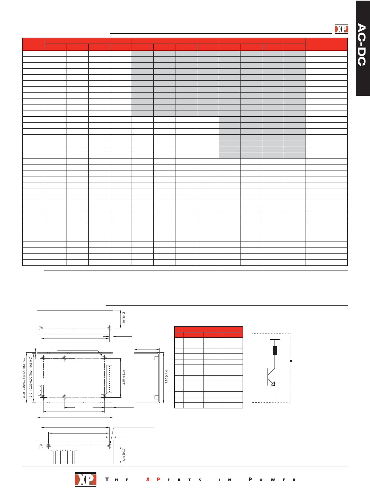
Mechanical Details
All dimensions are in inches (mm).
Weight: 0.77-0.99 lbs (350-450 g) approx.
For PCB-only version, overall dimensions are max 5.00 x 3.00 x 1.44 (127.0 x 76.2 x 36.6).
0.10 (2.5)
4.49 (114.3)
M3XP0.5 (Mounting Holes) X 4
0.25 (6.4)
1.54 (39.2)
AC P1
INPUT
L
N
G
P2
1
DC
OUTPUT
13
PFD
2.70 (68.6)
3.90 (99.06)
5.00 (127.0)
4.49 (114.3)
4.00 (101.6)
0.55 (14.0)
M3xP0.5 (Mounting Holes) X 3
0.25 (6.4)
PIN CONNECTIONS
Pin Single
Dual
Triple
1
V1
V2
V2
2
V1
V2
V2
3
V1
V1
V1
4
V1
V1
V1
5
V1
V1
V1
6
V1
V1
V1
7 Return Common Common
8 Return Common Common
9 Return Common Common
10 Return N/C
V3
11 Return Common Common
12 Return Common Common
13 PFD(1)
PFD(1)
PFD(1)
Power Fail Detect (PFD)
is +5 V for normal operation.
+5 V
Source current is 5 mA max.
Pin 13
PFD is <0.4 V for either
AC Fail (<90 VAC) or
DC Fail (<95% Vnom).
Sink current is 10 mA max.
Internal
Notes:
1. Optional Power Fail Detect signal on ‘P’ versions only. Standard models pin 13 is N/C.
2. I/P connector P1 mates with Molex housing 09-50-3051 & Molex 2878 series crimp terminal.
3. O/P P2 mates with Molex housing 09-50-3131 & Molex 2878 series crimp terminal.
4. For optional cover kit order part number SDS120 COVER†, to receive unit with cover fitted
add suffix ‘C’ to model number (overall height is 1.73 (44.0)).
5. For mating connector kit order part number SDS120 CON KIT†.
6. For cable harness order part number SDS120S LOOM† for single output models &
SDS120M LOOM† for multi-output models.
7. DIN clips are available for alternate mounting order 2 x ‘DIN CLIP’.
17-Apr-07
Share Link: 