TDA7550R_01 データシートの表示(PDF) - STMicroelectronics
部品番号
コンポーネント説明
メーカー
TDA7550R_01 Datasheet PDF : 10 Pages
| |||
TDA7550R
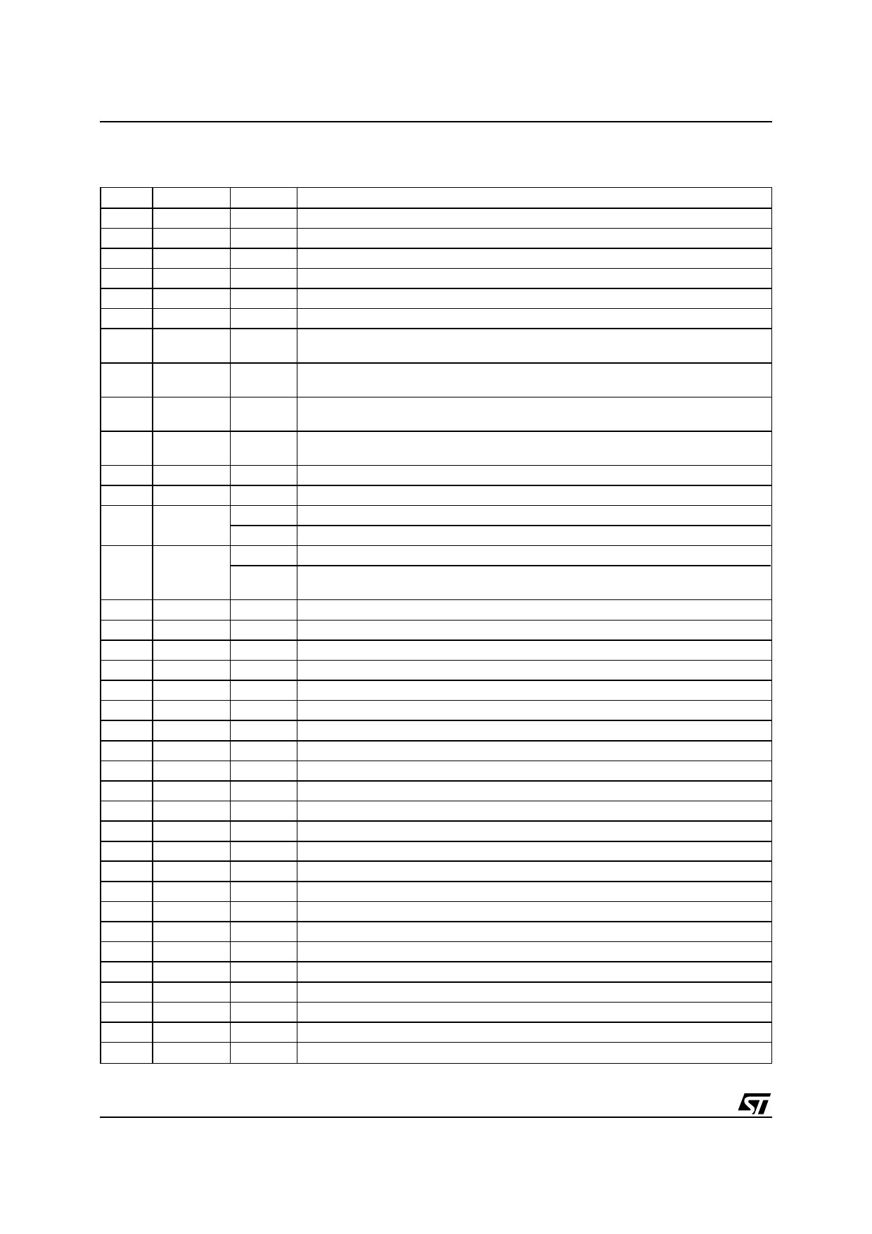
PIN FUNCTIONS (continued)
N.
Name
Type
Description
33
VDD
I
Digital power supply
34
GND
I
Ground
35
SDO
O
SAI Data Output
36
GPIO1
I/O
General Purpose I/O
37
GPIO0
I/O
General Purpose I/O
38
GPIO5
I/O
General Purpose I/O
39
DBCK
I/O
Debug port Bit Clock/Chip Status 1. The serial clock for the Debug Port is
provided. May also be used as GPIO9.
40
DBIN
I/O
Debug port Serial Input/Chip Status 0. The serial data input for the Debug Port is
provided. May also be used as GPIO11.
41
DBOUT
I/O
Debug Port Serial Output. This pin is the serial Data output for the Debug port.
May also be used as GPIO10.
42
DBRQN
I
Debug Port Request Input. This pin is used to request Debug Mode operation to
Euterpe
43 NRESET
I
System Reset. A low level applied to RESET input initializes the IC.
44
INTN
45 SCL/SCK
I
External interrupt line. When this line is asserted low the DSP may be interrupted.
I/O
I2C Serial Clock Line. Clock line for I2C bus. Schmitt trigger input.
46
SDA/SS
I/O
SPI Bit Clock. If SPI interface is enabled, it behaves as SPI bit clock.
I/O
I2C Serial Data Line. Data line for I2C bus. Schmitt trigger input.
I
SPI Slave Select. If SPI interface is enabled, it behaves as Slave select line for
SPI bus.
47
VDD
I
Digital Power Supply
48
GND
I
Ground
49
GPIO2
I/O
General Purpose I/O
50
GPIO6
I/O
General Purpose I/O
51
GPIO3
I/O
General Purpose I/O
52
GND
I
Ground
53
VDD
I
Digital Power Supply
54
VOUTR
O
Single-ended right channel analogue output from DAC
55
VOUTL
O
Single-ended left channel analogue output from DAC
56
CVDD
I
Digital Power supply for the internal CODEC cell
57
CGND
I
Ground for the internal CODEC cell
58
VINR
I
Single-ended right channel analogue input to ADC
59
VINL
I
Single-ended left channel analogue input to ADC
60
CGNDA
I
Ground for the internal CODEC cell
61
TEST4
O
Connect a 22K pull-down resistor
62
CVDDA
I
Power Supply for the internal CODEC cell
63
VREF
O
Voltage Reference from the CODEC cell
64 REFCAP
O
Voltage Reference Capacitor Bypass
65
GPIO7
I/O
General Purpose I/O
66
GPIO4
I/O
General Purpose I/O
67
VDD
I
Digital power supply
68 CLKOUT
O
Clock Output. Output Clock divided down from PLL
69
XTI
I
Crystal Oscillator Input. Crystal Oscillator Input drive
4/10
Share Link: 