MAX984CSE データシートの表示(PDF) - Maxim Integrated
部品番号
コンポーネント説明
メーカー
MAX984CSE Datasheet PDF : 17 Pages
| |||
Ultra-Low-Power, Open-Drain,
Single/Dual-Supply Comparators
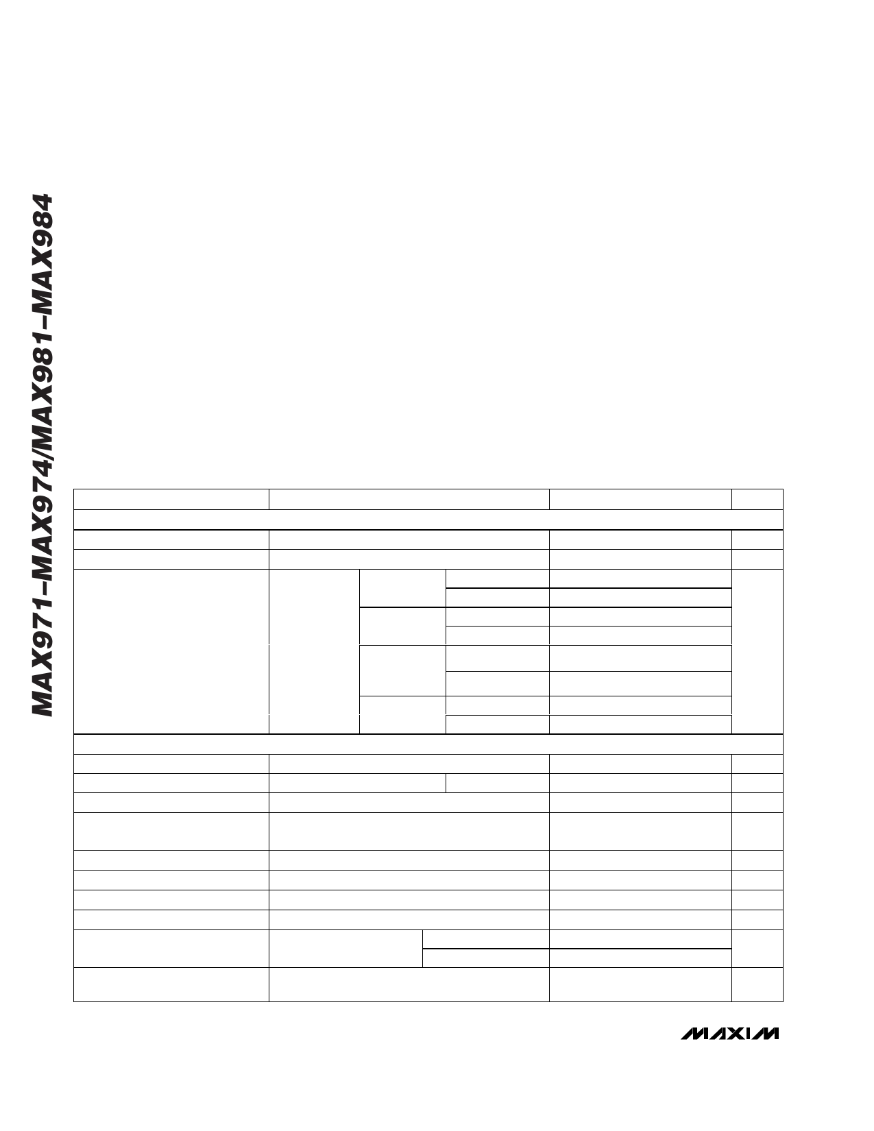
ABSOLUTE MAXIMUM RATINGS
V+ to V-, V+ to GND, GND to V-................................-0.3V, +12V
Inputs
Current: IN_+, IN_-, HYST..............................................20mA
Voltage: IN_+, IN_-, HYST ...............(V+ + 0.3V) to (V- - 0.3V)
Outputs
Current: REF...................................................................20mA
OUT_ ................................................................50mA
Voltage: REF ....................................(V+ + 0.3V) to (V- - 0.3V)
OUT_ (MAX9_1/9_4)..................12V to (GND - 0.3V)
(MAX9_2/9_3).......................12V to (V- - 0.3V)
OUT_ Short-Circuit Duration ..................................Continuous
Continuous Power Dissipation (TA = +70°C)
8-Bump UCSP (derate 4.7mW/°C above +70°C) ........379mW
8-Pin Plastic DIP (derate 9.09mW/°C above +70°C) ...727mW
8-Pin SO (derate 5.88mW/°C above +70°C)................471mW
8-Pin µMAX (derate 4.1mW/°C above +70°C) .............330mW
16-Pin Plastic DIP (derate 10.53mW/°C above +70°C)..842mW
16-Pin SO (derate 8.70mW/°C above +70°C) ................696mW
Operating Temperature Ranges
MAX97_C_ _/MAX98_C_ _ ..................................0°C to +70°C
MAX97_E_ _/MAX98_E_ _ ...............................-40°C to +85°C
Storage Temperature Range .............................-65°C to +150°C
Lead Temperature (soldering, 10s) .................................+300°C
Bump Temperature (soldering)
Reflow ..........................................................................+235°C
Stresses beyond those listed under “Absolute Maximum Ratings” may cause permanent damage to the device. These are stress ratings only, and functional
operation of the device at these or any other conditions beyond those indicated in the operational sections of the specifications is not implied. Exposure to
absolute maximum rating conditions for extended periods may affect device reliability.
ELECTRICAL CHARACTERISTICS—5V OPERATION
(V+ = 5V, V- = GND = 0V, TA = TMIN to TMAX, unless otherwise noted. Typical values are at TA = +25°C.) (Note 1)
PARAMETER
CONDITIONS
MIN
TYP
MAX UNITS
POWER REQUIREMENTS
Supply Voltage Range
(Note 2)
2.5
11
V
Output Voltage Range
Supply Current
0
MAX9_1,
TA = +25°C
HYST = REF C/E temp ranges
IN+ = IN- +
100mV
MAX972
MAX982/
MAX9_3,
HYST = REF
TA = +25°C
C/E temp ranges
TA = +25°C
C/E temp ranges
11
V
2.5
3.2
4
2.5
3.2
4
3.1
4.5
µA
6
MAX9_4
TA = +25°C
C/E temp ranges
5.5
6.5
8.5
COMPARATOR
Input Offset Voltage
Input Leakage Current (IN-, IN+)
Input Leakage Current (HYST)
VCM = 2.5V
IN+ = IN- = 2.5V
MAX9_1/MAX982/MAX9_3
C/E temp ranges
±10
mV
±0.01
±5
nA
±0.02
nA
Input Common-Mode Voltage
Range
V-
V+ - 1.3
V
Common-Mode Rejection Ratio
Power-Supply Rejection Ratio
V- to (V+ - 1.3V)
V+ = 2.5V to 11V
0.1
1.0
mV/V
0.1
1.0
mV/V
Voltage Noise
100Hz to 100kHz
20
Hysteresis Input Voltage Range MAX9_1/MAX982/MAX9_3
REF - 0.05
Response Time (High-to-Low
TA = +25°C, 100pF load, Overdrive = 10mV
12
Transition)
1MΩ pullup to V+
Overdrive = 100mV
4
Response Time (Low-to-High
Transition) (Note 3)
TA = +25°C, 100pF load, 1MΩ pullup to V+
300
µVRMS
REF
V
µs
µs
2 _______________________________________________________________________________________
Share Link: 