CL25N8-G データシートの表示(PDF) - Supertex Inc
部品番号
コンポーネント説明
メーカー
CL25N8-G Datasheet PDF : 5 Pages
| |||
CL25
Ordering Information
Device
Package Options
TO-92
TO-243AA (SOT-89)
CL25
CL25N3-G
CL25N8-G
-G indicates package is RoHS compliant (‘Green’)
Thermal Characteristics
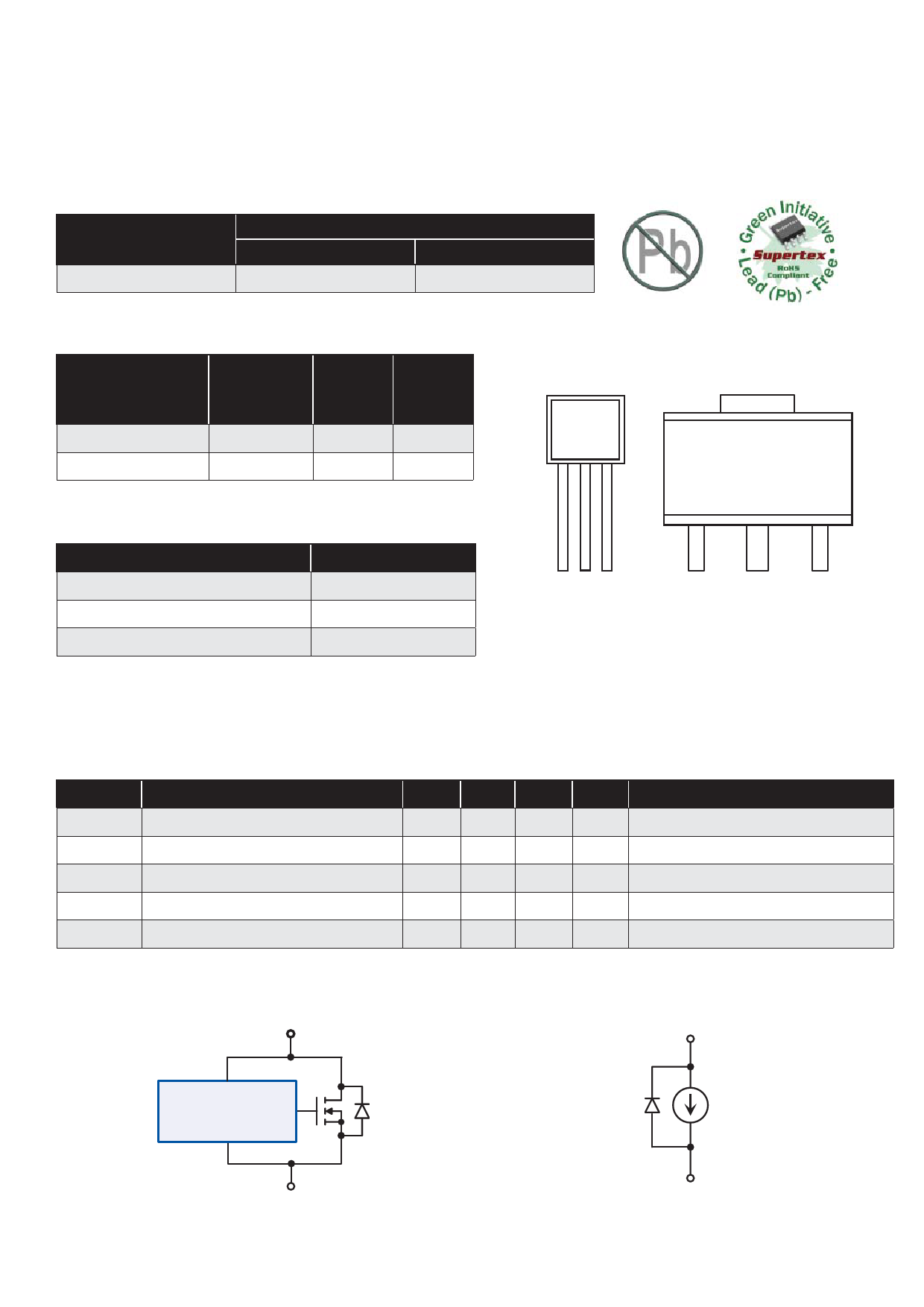
Pin Configuration
Package
Power
Dissipation
@TA = 25OC
θJC
OC/W
θJA
OC/W
VB
TO-92
0.6W
125
170
TO-243AA (SOT-89) 1.3W*
15
78*
* Mounted on FR4 board; 25mm x 25mm x 1.57mm
Absolute Maximum Ratings
Parameter
Value
Operating voltage, VA-B
100V
Operating junction temperature, TJ
-40°C to +125°C
Storage temperature, T
S
-55°C to +150°C
Absolute Maximum Ratings are those values beyond which damage to the device may
occur. Functional operation under these conditions is not implied. Continuous operation
of the device at the absolute rating level may affect device reliability. All voltages are
referenced to device ground.
VA NC VB
TO-92
(front view)
VA
VB
NC
TO-243AA
(top view)
NC = No Connect
Electrical Characteristics
(TJ=25°C unless otherwise specified)
Symbol Parameter
VA-B
IA-B
ΔIA-B/ΔT
TJ
RA-B
Operating voltage
Current regulation
IA-B temperature coefficient
Operating junction temperature
Dynamic resistance
Min
5
22.5
-
-40
-
Typ
-
25
0.01
-
300k
Max
90
27.5
-
125
-
Units Conditions
V ---
mA
%/OC
OC
VA-B = 5V - 90V
VA-B = 45V, TJ = -40OC to +100OC
---
Ω ---
Functional Circuit Diagram
VA
Equivalent Block Diagram
VA
Control Circuit
and Temperature
Compensation
VB
25mA
±10%
VB
2
Share Link: 