MAP3202SIRH データシートの表示(PDF) - MagnaChip Semiconductor
部品番号
コンポーネント説明
メーカー
MAP3202SIRH Datasheet PDF : 15 Pages
| |||
Confidential
Datasheet Version 1.1
Application Information
Current Mode Boost switching
regulator operation
The MAP3202 is operated in current mode PWM Boost
regulation method, which shows fast frequency response while
maintaining stable output voltage.
It features stable response by using the recommended
combination of resistor and capacitor at COMP and GND pin
for specific condition of wide input voltage, Output voltage and
variable Load condition.
Internal 5V Low Dropout Regulator
The MAP3202 has LDO embedded in it to supply Internal
analog, logic circuit and external REF Pin. This LDO operates
at a voltage level where Vcc is higher than the UVLO voltage. It
provides maximum 10mA of output current through regulator
which has 2% accuracy of performance.
To stabilize the voltage of REF Pin, it is recommended to use
low ESR capacitor which is as low as 1uF and connect it
between REF and GND Pin, and install it as close as to Pin.
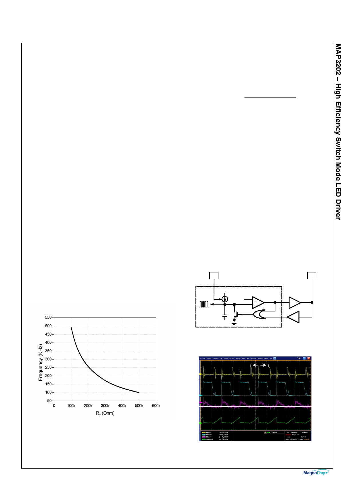
Boost Converter Switching Frequency
The MAP3202 can set the switching frequency of Boost
converter by connecting external resistor between RT and
GND Pin. Recommended switching frequency is 100 KHz to
400 KHz.
See Figure 1 for switching frequency adjustment resistor (RT)
The Boost switching frequency can be decided in the following
equation.
Tosc(us) = RT (Kohm) + 1.75
50
SYNCHRONIZATION
The MAP3202’s switching frequency can be set by internal
clock or by external master clock signal through SYNC Pin.
The clock signal of SYNC Pin needs to be faster than internal
Oscillator clock to ensure normal switching operation.
When synchronizing multiple MAP3202 on single board, all
SYNC Pin ICs of each device should be short to make all
devices in sync on the Oscillator clock of the fastest device.
It is recommended to use low ESR capacitor which is as low as
10pF and connect it between SYNC and GND Pin each device,
and install it as close as to Pin.
In this case, the number of synchronized devices differs
depending on the operation frequency of Oscillator.
If this function of peer to peer synchronization is not used, the
SYNC pin may be required to be open or short to GND. It is
recommended to connect SYNC Pin to GND because this
solution provides better immunity against parasitic noise from
layout.
RT
SYNC
67
78
REF
+
CK
OSCILLATOR
Figure 2 Internal OSC & SYNC circuit
Figure 1 Boost switching frequency vs. RT
March 2012
SYNC(4v/div)
Boost Drain(100V/div)
VO( AC 1V/div)
Iboost (0.5A/div)
300KHz/5%`
Figure 3 Synchronization by external clock
(Fixed 100 KHz 300 KHz)
Page 9
Share Link: 