MC74LVX541_11 データシートの表示(PDF) - ON Semiconductor
部品番号
コンポーネント説明
メーカー
MC74LVX541_11 Datasheet PDF : 7 Pages
| |||
MC74LVX541
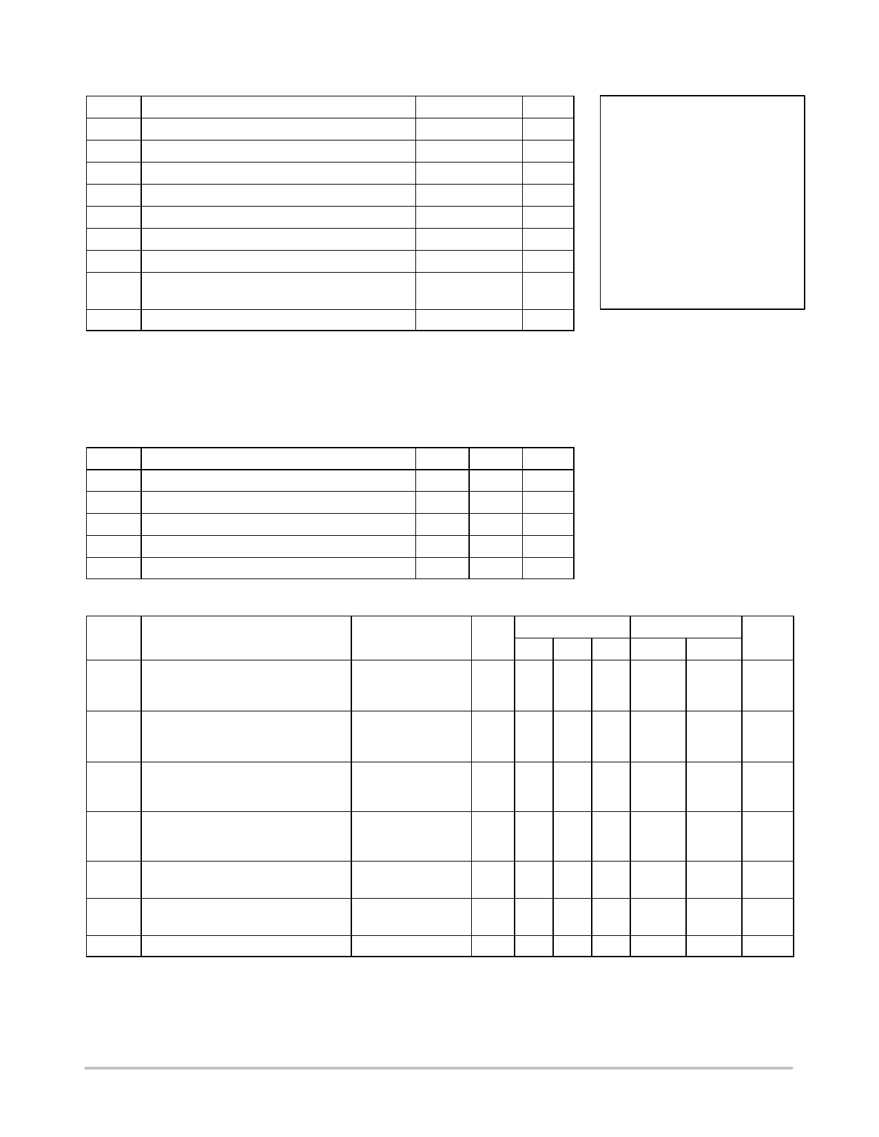
MAXIMUM RATINGS
Symbol
Parameter
Value
Unit
VCC DC Supply Voltage
– 0.5 to + 7.0
V
Vin DC Input Voltage
– 0.5 to + 7.0
V
Vout DC Output Voltage
– 0.5 to VCC + 0.5
V
IIK Input Diode Current
− 20
mA
IOK Output Diode Current
± 20
mA
Iout DC Output Current, per Pin
± 25
mA
ICC DC Supply Current, VCC and GND Pins
± 50
mA
PD Power Dissipation in Still Air,
SOIC Packages†
500
mW
TSSOP Package†
450
Tstg Storage Temperature
– 65 to + 150
°C
Stresses exceeding Maximum Ratings may damage the device. Maximum Ratings are stress
ratings only. Functional operation above the Recommended Operating Conditions is not implied.
Extended exposure to stresses above the Recommended Operating Conditions may affect device
reliability.
†Derating — SOIC Packages: – 7 mW/°C from 65° to 125°C
TSSOP Package: − 6.1 mW/°C from 65° to 125°C
This device contains protection
circuitry to guard against damage
due to high static voltages or electric
fields. However, precautions must
be taken to avoid applications of any
voltage higher than maximum rated
voltages to this high−impedance cir-
cuit. For proper operation, Vin and
Vout should be constrained to the
range GND v (Vin or Vout) v VCC.
Unused inputs must always be
tied to an appropriate logic voltage
level (e.g., either GND or VCC).
Unused outputs must be left open.
RECOMMENDED OPERATING CONDITIONS
Symbol
Parameter
Min
VCC DC Supply Voltage
2.0
Vin DC Input Voltage
0
Vout DC Output Voltage
0
TA Operating Temperature, All Package Types
−40
tr, tf Input Rise and Fall Time
VCC = 3.3V ±0.3V
0
Max
3.6
5.5
VCC
+ 85
100
Unit
V
V
V
°C
ns/V
DC ELECTRICAL CHARACTERISTICS
Symbol
Parameter
VIH Minimum High−Level Input Voltage
Test Conditions
VIL Maximum Low−Level Input Voltage
VOH Minimum High−Level Output Voltage IOH = − 50 mA
Vin = VIH or VIL
IOH = − 50 mA
IOH = − 4 mA
VOL Maximum Low−Level Output Voltage IOL = 50 mA
Vin = VIH or VIL
IOL = 50 mA
IOL = 4 mA
Iin
Maximum Input Leakage Current
Vin = 5.5 V or GND
IOZ Maximum Three−State Leakage
Current
Vin = VIL or VIH
Vout = VCC or GND
ICC Maximum Quiescent Supply Current Vin = VCC or GND
VCC
TA = 25°C
TA = − 40 to 85°C
V Min Typ Max Min
Max
Unit
2.0 1.50
3.0 2.0
3.6 2.4
1.50
V
2.0
2.4
2.0
0.50
0.50
V
3.0
0.80
0.80
3.6
0.80
0.80
2.0 1.9 2.0
1.9
V
3.0 2.9 3.0
2.9
3.0 2.58
2.48
2.0
0.0 0.1
3.0
0.0 0.1
3.0
0.36
0.1
V
0.1
0.44
0 to
±0.1
±1.0
mA
3.6
3.6
±0.2
±2.5
mA
5
3.6
4.0
40.0
mA
http://onsemi.com
3
Share Link: 