AM28F512 データシートの表示(PDF) - Advanced Micro Devices
部品番号
コンポーネント説明
メーカー
AM28F512 Datasheet PDF : 35 Pages
| |||
VCC < VLKO (see DC Characteristics section for
voltages). When VCC < VLKO, the command register is
disabled, all internal program/erase circuits are
disabled, and the device resets to the read mode. The
device ignores all writes until VCC > VLKO. The user
must ensure that the control pins are in the correct logic
state when VCC > VLKO to prevent uninitentional writes.
Write Pulse “Glitch” Protection
Noise pulses of less than 10 ns (typical) on OE#, CE#
or WE# will not initiate a write cycle.
Logical Inhibit
Writing is inhibited by holding any one of OE# = VIL, CE#
= VIH or WE# = VIH. To initiate a write cycle CE# and
WE# must be a logical zero while OE# is a logical one.
Power-Up Write Inhibit
Power-up of the device with WE# = CE# = VIL and
OE# = VIH will not accept commands on the rising
edge of WE#. The internal state machine is automat-
ically reset to the read mode on power-up.
FUNCTIONAL DESCRIPTION
Description of User Modes
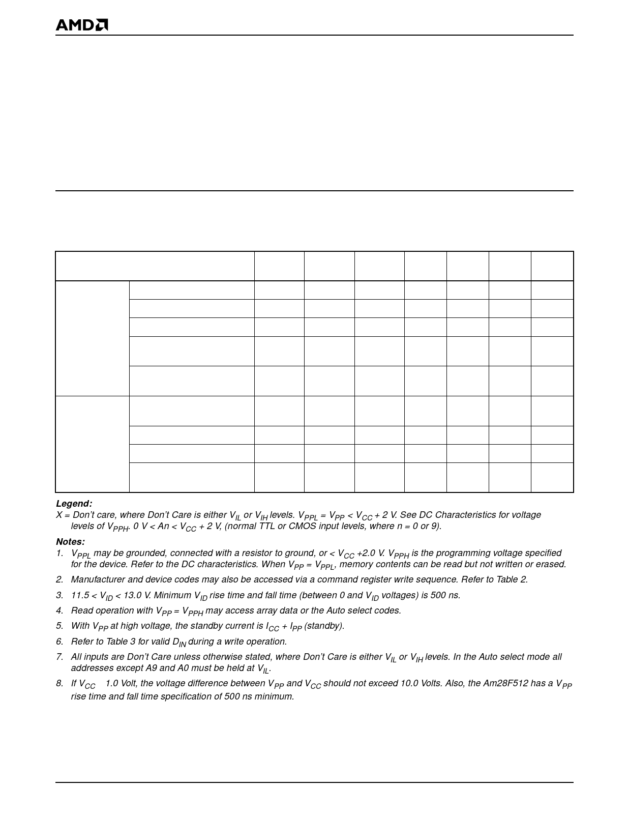
Table 1. Am28F512 User Bus Operations (Notes 7 and 8)
Read-Only
Operation
Read
Standby
Output Disable
Auto-select Manufacturer
Code (Note 2)
Auto-select Device Code
(Note 2)
Read
VPP
CE# (E#) OE# (G#) WE# (W#) (Note 1) A0
A9
I/O
VIL
VIL
X
VPPL
A0
A9
DOUT
VIH
X
X
VPPL
X
X
HIGH Z
VIL
VIH
VIH
VPPL
X
X
HIGH Z
VIL
VIL
VIH
VPPL
VIL
VID
CODE
(Note 3) (01H)
VIL
VIL
VIH
VPPL
VIH
VID
CODE
(Note 3) (25H)
VIL
VIL
VIH
VPPH
A0
A9
DOUT
(Note 4)
Read/Write
Standby (Note 5)
Output Disable
Write
VIH
X
X
VPPH
X
X
HIGH Z
VIL
VIH
VIH
VPPH
X
X
HIGH Z
VIL
VIH
VIL
VPPH
A0
A9
DIN
(Note 6)
Legend:
X = Don’t care, where Don’t Care is either VIL or VIH levels. VPPL = VPP < VCC + 2 V. See DC Characteristics for voltage
levels of VPPH. 0 V < An < VCC + 2 V, (normal TTL or CMOS input levels, where n = 0 or 9).
Notes:
1. VPPL may be grounded, connected with a resistor to ground, or < VCC +2.0 V. VPPH is the programming voltage specified
for the device. Refer to the DC characteristics. When VPP = VPPL, memory contents can be read but not written or erased.
2. Manufacturer and device codes may also be accessed via a command register write sequence. Refer to Table 2.
3. 11.5 < VID < 13.0 V. Minimum VID rise time and fall time (between 0 and VID voltages) is 500 ns.
4. Read operation with VPP = VPPH may access array data or the Auto select codes.
5. With VPP at high voltage, the standby current is ICC + IPP (standby).
6. Refer to Table 3 for valid DIN during a write operation.
7. All inputs are Don’t Care unless otherwise stated, where Don’t Care is either VIL or VIH levels. In the Auto select mode all
addresses except A9 and A0 must be held at VIL.
8. If VCC ≤ 1.0 Volt, the voltage difference between VPP and VCC should not exceed 10.0 Volts. Also, the Am28F512 has a VPP
rise time and fall time specification of 500 ns minimum.
8
Am28F512
Share Link: 