A2580 データシートの表示(PDF) - Allegro MicroSystems
部品番号
コンポーネント説明
メーカー
A2580 Datasheet PDF : 12 Pages
| |||
2580, 2585, AND 2588
8-CHANNEL
SOURCE DRIVERS
UDN2580A and A2580SLW
ELECTRICAL CHARACTERISTICS at TA = +25°C, VS = 0 V, VEE = -45 V (unless otherwise noted).
Characteristic
Output Leakage
Current
Output Sustaining
Voltage
Symbol
ICEX
VCE(SUS)
Test Conditions
VlN = -0.5 V, VOUT = VEE = -50 V
VlN = -0.4 V, VOUT = VEE = -50 V, TA = 70°C
VlN = -0.4 V, IOUT = -25 mA, Note 1
Min.
—
—
35
Limits
Max.
50
100
—
Units
µA
µA
V
Output Saturation
Voltage
Input Current
Input Voltage
Clamp Diode
Leakage Current
Clamp Diode
Forward Voltage
VCE(SAT)
IIN(ON)
IIN(OFF)
VIN(ON)
VIN(OFF)
IR
VF
VlN = -2.4 V, IOUT = -100 mA
VlN = -3.0 V, IOUT = -225 mA
VlN = -3.6 V, IOUT = -350 mA
VlN = -3.6 V, IOUT = -350 mA
VlN = -15 V, IOUT = -350 mA
IOUT = -500 µA, TA = 70°C, Note 3
IOUT = -100 mA, VCE ≤1.8 V, Note 4
IOUT = -225 mA, VCE ≤1.9 V, Note 4
IOUT = -350 mA, VCE ≤2.0 V, Note 4
IOUT = -500 µA, TA = 70°C
VR = 50 V, TA = 70°C
IF = 350 mA
—
1.8
V
—
1.9
V
—
2.0
V
—
-500
µA
—
-2.1
mA
-50
—
µA
—
-2.4
V
—
-3.0
V
—
-3.6
V
-0.2
—
V
—
50
µA
—
2.0
V
Input Capacitance
Turn-On Delay
Turn-Off Delay
CIN
tPHL
tPLH
0.5 EIN to 0.5 EOUT
0.5 EIN to 0.5 EOUT
—
25
pF
—
5.0
µs
—
5.0
µs
NOTES:
1. Pulsed test, tp ≤ 300 µs,
duty cycle ≤ 2%.
2. Negative current is
defined as coming out of the
specified device pin.
3. The IIN(OFF) current limit
guarantees against partial
turn-on of the output.
4. The VIN(ON) voltage limit
guarantees a minimum
output source current per the
specified conditions.
5. The substrate must
always be tied to the most
negative point and must be at
least 4.0 V below VS.
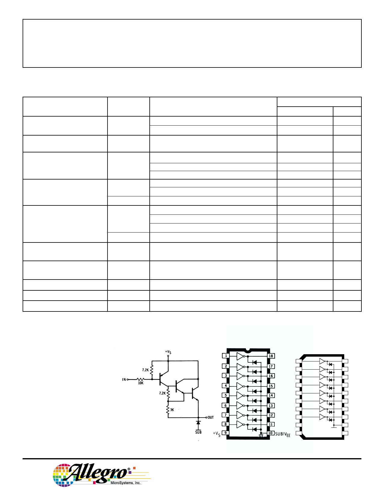
PARTIAL SCHEMATIC
Dwg. No. A-11,358
UDN2580A
A2580SLW
1
2
3
4
5
6
7
8
+VS 9
10 NC
Dwg. No. A-11,359
20
19
18
17
16
15
14
13
12
SUB
NC 11
SUB/VEE
Dwg. PP-064
115 Northeast Cutoff, Box 15036
4
Worcester, Massachusetts 01615-0036 (508) 853-5000
Share Link: 