AG402-86G データシートの表示(PDF) - TriQuint Semiconductor
部品番号
コンポーネント説明
メーカー
AG402-86G Datasheet PDF : 5 Pages
| |||
AG402-86
InGaP HBT Gain Block
Product Features
• DC – 6000 MHz
• 15 dB Gain @ 900 MHz
• +17 dBm P1dB @ 900 MHz
• +32.5 dBm OIP3 @ 900 MHz
• Single Voltage Supply
• Internally matched to 50 Ω
• Robust 1000V ESD, Class 1C
• Lead-free/green/RoHS-compliant
SOT-363 package
Applications
• Mobile Infrastructure
• CATV / FTTX
• WLAN / ISM
• RFID
• WiMAX / WiBro
Product Description
The AG402-86 is a general-purpose buffer amplifier that
offers high dynamic range in a low-cost surface-mount
package. At 900 MHz, the AG402-86 typically provides
15 dB gain, +32.5 dBm OIP3, and +17 dBm P1dB. The
device combines dependable performance with consistent
quality to maintain MTTF values exceeding 1000 years at
mounting temperatures of +85 °C and is housed in a lead-
free/green/RoHS-compliant SOT-86 (micro-X) industry-
standard SMT package.
The AG402-86 consists of a Darlington-pair amplifier
using the high reliability InGaP/GaAs HBT process
technology and only requires DC-blocking capacitors, a
bias resistor, and an inductive RF choke for operation.
The broadband MMIC amplifier can be directly applied to
various current and next generation wireless technologies
such as GPRS, GSM, CDMA, and W-CDMA. In addition,
the AG402-86 will work for other various applications
within the DC to 6 GHz frequency range such as CATV
and WiMAX.
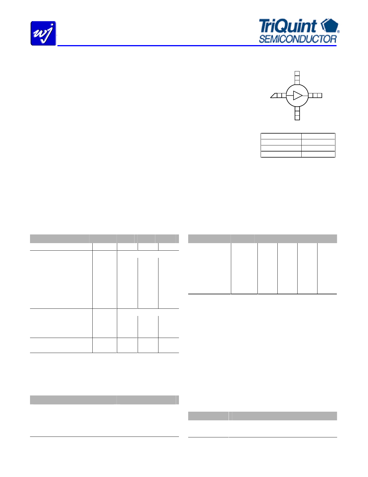
Functional Diagram
GND
4
RF In 1
3 RF Out
2
GND
Function
Input
Output/Bias
Ground
Pin No.
1
3
2, 4
Specifications (1)
Parameter
Operational Bandwidth
Test Frequency
Gain
Input Return Loss
Output Return Loss
Output P1dB
Output IP3 (2)
Output IP2
Noise Figure
Test Frequency
Gain
Output P1dB
Output IP3 (2)
Device Voltage
Device Current
Units
MHz
MHz
dB
dB
dB
dBm
dBm
dBm
dB
MHz
dB
dBm
dBm
V
mA
Min
DC
13.3
Typ
900
15.0
18
25
+17.1
+32.6
+46
3.7
1900
14.3
+15.9
+29.6
4.91
60
Max
6000
15.3
1. Test conditions: T = 25 ºC, Supply Voltage = +6 V, Rbias = 18.2 Ω, 50 Ω System.
2. 3OIP measured with two tones at an output power of 0 dBm/tone separated by 10 MHz. The
suppression on the largest IM3 product is used to calculate the 3OIP using a 2:1 rule.
Typical Performance (1)
Parameter
Frequency
S21
S11
S22
Output P1dB
Output IP3
Noise Figure
Units
MHz
dB
dB
dB
dBm
dBm
dB
500
15.2
-16
-28
+17.1
+33.3
3.7
Typical
900 1900
15.0 14.3
-18 -20
-25 -16
+17.1 +15.9
+32.6 +29.6
3.7 3.9
2140
14.0
-20
-16
+15.3
+28.2
3.9
Absolute Maximum Rating
Parameter
Storage Temperature
DC Voltage
RF Input Power (continuous)
Thermal Resistance, Rth
Junction Temperature
Rating
-55 to +125 °C
+5 V
+10 dBm
216°C/W
+177°C
Operation of this device above any of these parameters may cause permanent damage.
Ordering Information
Part No.
AG402-86G
AG402-86PCB
Description
InGaP HBT Gain Block
(lead-free/green/RoHS-compliant SOT-86 Package)
700 – 2400 MHz Fully Assembled Eval. Board
Standard tape / reel size = 3000 pieces on a 13” reel
Specifications and information are subject to change without notice
WJ Communications, Inc • Phone 1-800-WJ1-4401 • FAX: 408-577-6621 • e-mail: sales@wj.com • Web site: www.wj.com, www.TriQuint.com
Page 1 of 5 March 2008
Share Link: 