74LV541PW データシートの表示(PDF) - NXP Semiconductors.
部品番号
コンポーネント説明
メーカー
74LV541PW Datasheet PDF : 15 Pages
| |||
NXP Semiconductors
74LV541
Octal buffer/line driver; 3-state
Table 7. Dynamic characteristics …continued
Voltages are referenced to GND (ground = 0 V). For test circuit see Figure 7.
Symbol Parameter
Conditions
−40 °C to +85 °C
Min Typ[1] Max
CPD
power dissipation CL = 50 pF; fi = 1 MHz;
capacitance
VI = GND to VCC
[4]
-
37
-
[1] All typical values are measured at Tamb = 25 °C.
[2] tpd is the same as tPLH and tPHL.
ten is the same as tPZL and tPZH.
tdis is the same as tPLZ and tPHZ.
[3] Typical values are measured at nominal supply voltage (VCC = 3.3 V).
[4] CPD is used to determine the dynamic power dissipation (PD in µW).
PD = CPD × VCC2 × fi × N + Σ(CL × VCC2 × fo) where:
fi = input frequency in MHz, fo = output frequency in MHz
CL = output load capacitance in pF
VCC = supply voltage in Volts
N = number of inputs switching
Σ(CL × VCC2 × fo) = sum of the outputs.
−40 °C to +125 °C Unit
Min
Max
-
-
pF
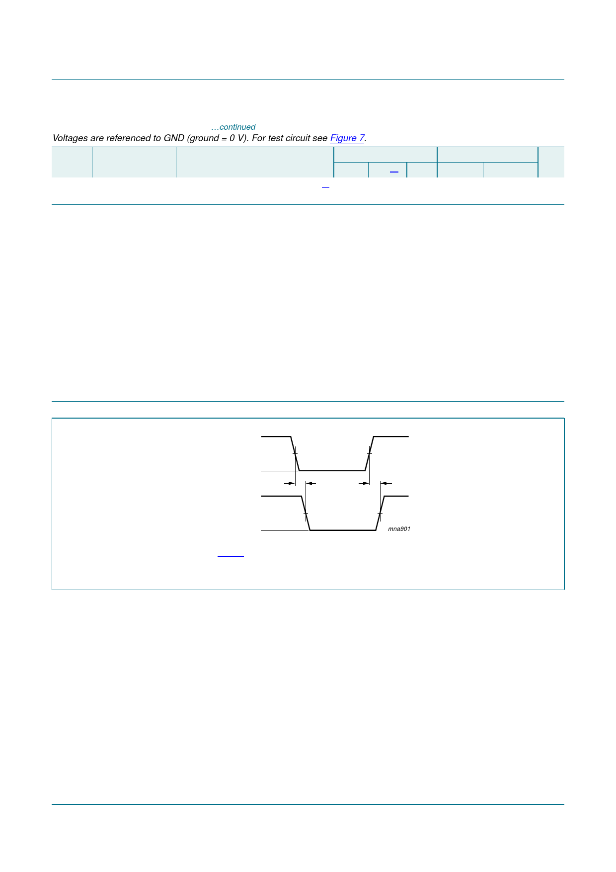
11. Waveforms
VI
An input
GND
VOH
Yn output
VOL
VM
t PHL
VM
t PLH
mna901
Fig 5.
Measurement points are given in Table 8.
VOL and VOH are typical voltage output levels that occur with the output load.
Propagation delay input (An) to output (Yn)
74LV541_3
Product data sheet
Rev. 03 — 14 April 2009
© NXP B.V. 2009. All rights reserved.
6 of 15
Share Link: 