LC75814V データシートの表示(PDF) - ON Semiconductor
部品番号
コンポーネント説明
メーカー
LC75814V Datasheet PDF : 15 Pages
| |||
LC75814V
Specifications
Absolute Maximum Ratings at Ta = 25°C, VSS = 0 V
Parameter
Maximum supply voltage
Input voltage
Output voltage
Output current
Allowable power dissipation
Operating temperature
Storage temperature
Symbol
VDD max
VLCD max
VIN 1
VIN 2
VIN 3
VOUT 1
VOUT 2
IOUT 1
IOUT 2
IOUT 3
Pd max
Topr
Tstg
Conditions
VDD
VLCD
CE, CL, DI, INH
OSC
VLCD 1, VLCD 2
OSC
S1 to S16, COM1 to COM4, P1 to P4
S1 to S16
COM1 to COM4
P1 to P4
Ta = 85°C
Ratings
Unit
–0.3 to +7.0
V
–0.3 to +7.0
V
–0.3 to +7.0
V
–0.3 to VDD + 0.3
V
–0.3 to VLCD + 0.3
V
–0.3 to VDD + 0.3
V
–0.3 to VLCD + 0.3
V
300
μA
3
mA
5
mA
100
mW
–40 to +85
°C
–55 to +125
°C
Stresses exceeding those listed in the Maximum Ratings table may damage the device. If any of these limits are exceeded, device functionality should not be assumed,
damage may occur and reliability may be affected.
Allowable Operating Ranges at Ta = –40 to +85°C, VSS = 0 V
Parameter
Supply voltage
Input voltage
Input high level voltage
Input low level voltage
Recommended external resistance
Recommended external capacitance
Guaranteed oscillation range
Data setup time
Data hold time
CE wait time
CE setup time
CE hold time
High level clock pulse width
Low level clock pulse width
Rise time
Fall time
INH switching time
Symbol
VDD
VLCD
VLCD1
VLCD2
VIH
VIL
ROSC
COSC
fOSC
tds
tdh
tcp
tcs
tch
tøH
tøL
tr
tf
tc
Conditions
VDD
VLCD
VLCD1
VLCD2
CE, CL, DI, INH
CE, CL, DI, INH
OSC
OSC
OSC
CL, DI: Figure 2
CL, DI: Figure 2
CE, CL: Figure 2
CE, CL: Figure 2
CE, CL: Figure 2
CL: Figure 2
CL: Figure 2
CE, CL, DI: Figure 2
CE, CL, DI: Figure 2
INH, CE: Figure 3
min
2.7
2.7
0.8 VDD
0
25
160
160
160
160
160
160
160
10
Ratings
typ
2/3 VLCD
1/3 VLCD
43
680
50
160
160
max
Unit
6.0
V
6.0
V
VLCD
V
VLCD
V
6.0
V
0.2 VDD
V
k
pF
100
kHz
ns
ns
ns
ns
ns
ns
ns
ns
ns
μs
Functional operation above the stresses listed in the Recommended Operating Ranges is not implied. Extended exposure to stresses beyond the Recommended
Operating Ranges limits may affect device reliability.
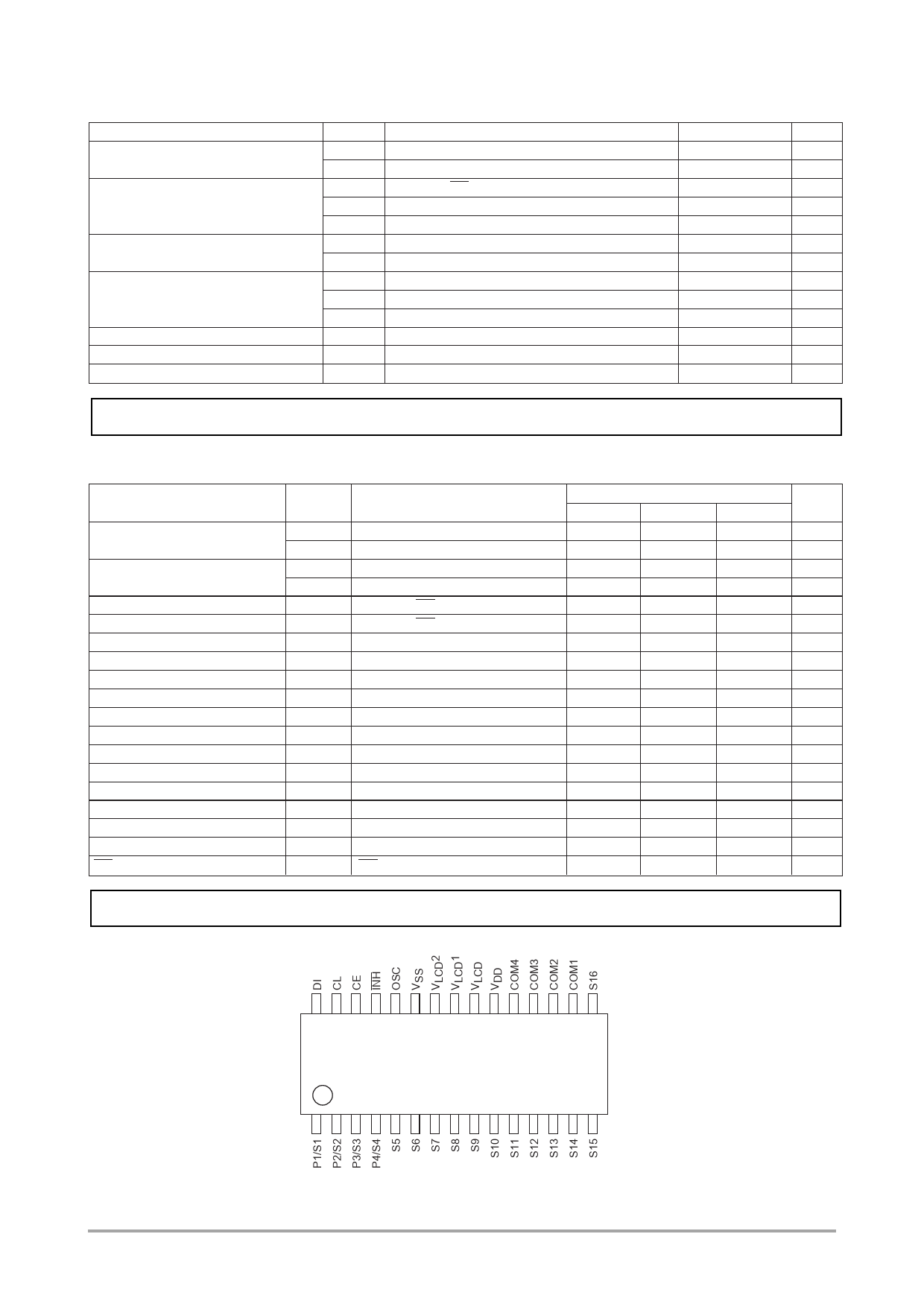
Pin Assignment
LC75814V
Top view
www.onsemi.com
2
Share Link: 