ADC0803 データシートの表示(PDF) - Renesas Electronics
部品番号
コンポーネント説明
メーカー
ADC0803 Datasheet PDF : 17 Pages
| |||
ADC0803, ADC0804
IC voltage regulators may be used for references if the ambient
temperature changes are not excessive.
Zero Error
The zero of the A/D does not require adjustment. If the minimum
analog input voltage value, VlN(MlN), is not ground, a zero offset
can be done. The converter can be made to output 0000 0000
digital code for this minimum input voltage by biasing the A/D
VIN(-) input at this VlN(MlN) value (see Applications section). This
utilizes the differential mode operation of the A/D.
The zero error of the A/D converter relates to the location of the
first riser of the transfer function and can be measured by
grounding the VIN(-) input and applying a small magnitude
positive voltage to the VIN(+) input. Zero error is the difference
between the actual DC input voltage which is necessary to just
cause an output digital code transition from 0000 0000 to 0000
0001 and the ideal 1/2 LSB value (1/2 LSB = 9.8mV for VREF/2 =
2.500V).
Full Scale Adjust
The full scale adjustment can be made by applying a
differential input voltage which is 11/2 LSB down from the
desired analog full scale voltage range and then adjusting the
magnitude of the VREF/2 input (pin 9) for a digital output code
which is just changing from 1111 1110 to 1111 1111. When
offsetting the zero and using a span-adjusted VREF/2 voltage,
the full scale adjustment is made by inputting VMlN to the VIN(-
) input of the A/D and applying a voltage to the VIN(+) input
which is given by:
VIN+fSADJ
=
VMAX – 1.5
---V----M-----A----X-----–----V-----M----I--N-----
256
,
where:
VMAX = the high end of the analog input range, and
VMIN = the low end (the offset zero) of the analog range. (Both
are ground referenced.)
Clocking Option
The clock for the A/D can be derived from an external source
such as the CPU clock or an external RC network can be
added to provIde self-clocking. The CLK IN (pin 4) makes use
of a Schmitt trigger as shown in Figure 16.
CLK R
R
CLK IN
C
19
ADC0803-
ADC0804
fCLK
1
1.1 RC
R 10k
4
CLK
FIGURE 16. SELF-CLOCKING THE A/D
Heavy capacitive or DC loading of the CLK R pin should be
avoided as this will disturb normal converter operation. Loads
less than 50pF, such as driving up to 7 A/D converter clock
inputs from a single CLK R pin of 1 converter, are allowed. For
larger clock line loading, a CMOS or low power TTL buffer or
PNP input logic should be used to minimize the loading on the
CLK R pin (do not use a standard TTL buffer).
Restart During a Conversion
If the A/D is restarted (CS and WR go low and return high)
during a conversion, the converter is reset and a new
conversion is started. The output data latch is not updated if
the conversion in progress is not completed. The data from the
previous conversion remain in this latch.
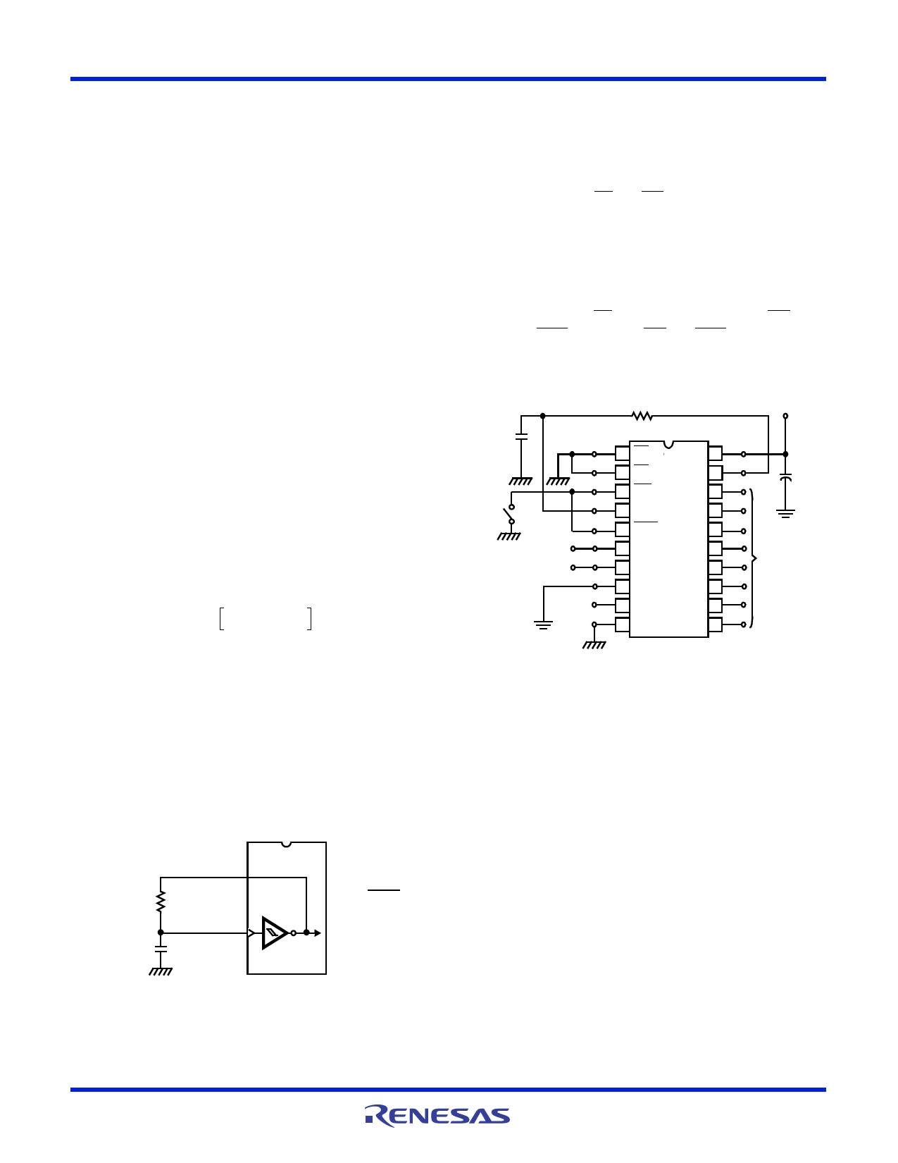
Continuous Conversions
In this application, the CS input is grounded and the WR input
is tied to the INTR output. This WR and INTR node should be
momentarily forced to logic low following a power-up cycle to
insure circuit operation. See Figure 17 for details.
150pF
N.O.
START
ANALOG
INPUTS
10K
ADC0803 - ADC0804
1 CS
V+ 20
2 RD CLK R 19
3 WR
4 CLK IN
5 INTR
6 VIN (+)
7 VIN (-)
8 AGND
9 VREF/2
10 DGND
DB0 18
DB1 17
DB2 16
DB3 15
DB4 14
DB5 13
DB6 12
DB7 11
5V (VREF)
+
10F
LSB
DATA
OUTPUTS
MSB
FIGURE 17. FREE-RUNNING CONNECTION
Driving the Data Bus
This CMOS A/D, like MOS microprocessors and memories, will
require a bus driver when the total capacitance of the data bus
gets large. Other circuItry, which is tied to the data bus, will add
to the total capacitive loading, even in three-state (high-
impedance mode). Back plane busing also greatly adds to the
stray capacitance of the data bus.
There are some alternatives available to the designer to
handle this problem. Basically, the capacitive loading of the
data bus slows down the response time, even though DC
specifications are still met. For systems operating with a
relatively slow CPU clock frequency, more time is available in
which to establish proper logic levels on the bus and
therefore higher capacitive loads can be driven (see Typical
Performance Curves).
At higher CPU clock frequencies time can be extended for I/O
reads (and/or writes) by inserting wait states (8080) or using
clock-extending circuits (6800).
FN3094 Rev 4.00
August 2002
Page 11 of 17
Share Link: 