AD7545UE データシートの表示(PDF) - Analog Devices
部品番号
コンポーネント説明
メーカー
AD7545UE Datasheet PDF : 9 Pages
| |||
AD7545
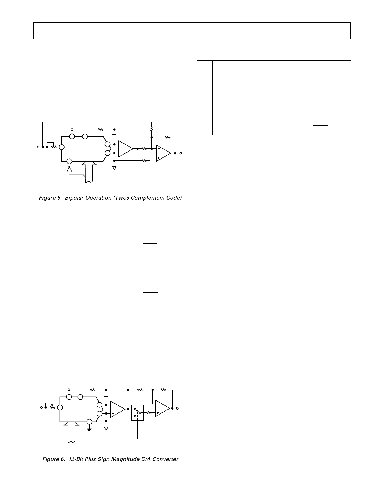
Figure 5 and Table III illustrate the recommended circuit and
code relationship for bipolar operation. The D/A function itself
uses offset binary code and inverter U1 on the MSB line con-
verts twos complement input code to offset binary code. If ap-
propriate; inversion of the MSB may be done in software using
an exclusive –OR instruction and the inverter omitted. R3, R4
and R5 must be selected to match within 0.01% and they should
be the same type of resistor (preferably wire-wound or metal
foil), so their temperature coefficients match. Mismatch of R3
value to R4 causes both offset and full-scale error. Mismatch of
R5 and R4 and R3 causes full-scale error.
VDD
R2*
18
20
C1
33pF
R4
20kΩ
VDD
RFB
OUT1 1
VIN
19 VREF
R1*
AD7545
AGND 2
DB11
4
DB10–DB0
A1
AD544L
R3
10kΩ
R6
5kΩ
R5
20kΩ
A2
AD544J
VOUT
10%
U1
(SEE TEXT)
11
ANALOG
COMMON
12
*FOR VALUES OF R1 AND R2
DATA INPUT
SEE TABLE I.
Figure 5. Bipolar Operation (Twos Complement Code)
Table III. Twos Complement Code Table for Circuit of
Figure 5
Data Input
0111 1111 1111
0000 0000
0000 0000
1111 1111
0001
0000
1111
1000 0000 0000
Analog Output
2047
+VIN × 2048
1
+VIN × 2048
0 Volts
1
–VIN × 2048
2048
–VIN × 2048
Figure 6 shows an alternative method of achieving bipolar out-
put. The circuit operates with sign plus magnitude code and has
the advantage of giving 12-bit resolution in each quadrant, com-
pared with 11-bit resolution per quadrant for the circuit of Fig-
ure 5. The AD7592 is a fully protected CMOS change-over
switch with data latches. R4 and R5 should match each other to
0.01% to maintain the accuracy of the D/A converter. Mismatch
between R4 and R5 introduces a gain error.
VDD
R2*
18
20
VDD
RFB OUT1 1
VIN
R1* 19 VREF AD7545
AGND 2
DB11–DB0
3
12
SIGN BIT
C1
33pF
A1
AD544L
ANALOG
COMMON
R4
20kΩ
R5
20kΩ
R3
10kΩ
10%
VOUT
A2
AD544J
1/2 AD7592JN
*FOR VALUES OF R1 AND R2
SEE TABLE I.
Table IV. 12-Plus Sign Magnitude Code Table for Circuit of
Figure 6
Sign Binary Number in DAC
Bit MSB
LSB
Analog Output, VOUT
0
1111 1111 1111
0
0000 0000 0000
1
0000 0000 0000
1
1111 1111 1111
Note: Sign bit of “0” connects R3 to GND.
4095
+ VIN × 4096
0 Volts
0 Volts
4095
– VIN × 4096
APPLICATIONS HINTS
Output Offset: (CMOS D/A converters exhibit a code depen-
dent output resistance which, in turn, causes a code dependent
amplifier noise gain. The effect is a code dependent differential
nonlinearity term at the amplifier output that depends on VOS
where VOS is the amplifier input offset voltage. To maintain
monotonic operation it is recommended that VOS be no greater
than 25 × 10–6) (VREF) over the temperature range of operation.
Suitable op amps are AD517L and AD544L. The AD517L is
best suited for fixed reference applications with low bandwidth
requirements: it has extremely low offset (50 µV) and in most
applications will not require an offset trim. The AD544L has a
much wider bandwidth and higher slew rate and is recommended
for multiplying and other applications requiring fast settling. An
offset trim on the AD544L may be necessary in some circuits.
General Ground Management: AC or transient voltages
between AGND and DGND can cause noise injection into the
analog output. The simplest method of ensuring that voltages at
AGND and DGND are equal is to tie AGND and DGND
together at the AD7545. In more complex systems where the
AGND and DGND intertie is on the backplane, it is recom-
mended that two diodes be connected in inverse parallel
between the AD7545 AGND and DGND pins (IN914 or
equivalent).
Digital Glitches: When WR and CS are both low the latches
are transparent and the D/A converter inputs follow the data
inputs. In some bus systems, data on the data bus is not always
valid for the whole period during which WR is low and as a
result invalid data can briefly occur at the D/A converter inputs
during a write cycle. Such invalid data can cause unwanted
glitches at the output of the D/A converter. The solution to this
problem, if it occurs, is to retime the write pulse WR so that it
only occurs when data is valid.
Another cause of digital glitches is capacitive coupling from the
digital lines to the OUT1 and AGND terminals. This should be
minimized by screening the analog pins of the AD7545 (Pins 1,
2, 19, 20) from the digital pins by a ground track run between
Pins 2 and 3 and between Pins 18 and 19 of the AD7545. Note
how the analog pins are at one end of the package and separated
from the digital pins by VDD and DGND to aid screening at
the board level. On-chip capacitive coupling can also give rise
to crosstalk from the digital-to-analog sections of the AD7545,
particularly in circuits with high currents and fast rise and
fall times. This type of crosstalk is minimized by using
Figure 6. 12-Bit Plus Sign Magnitude D/A Converter
REV. A
–5–
Share Link: 