548G-05 データシートの表示(PDF) - Integrated Device Technology
部品番号
コンポーネント説明
メーカー
548G-05 Datasheet PDF : 7 Pages
| |||
ICS548-05
T1/E1 CLOCK MULTIPLIER
CLOCK SYNTHESIZER
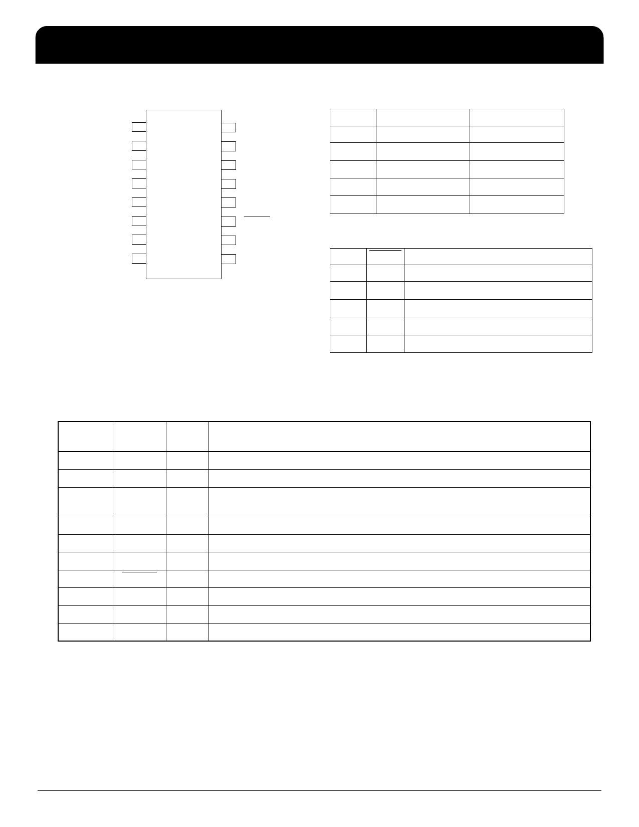
Pin Assignment
X1/ICLK
1
VDD
2
VDD
3
REFEN
4
GND
5
GND
6
GND
7
VDD
8
16
X2
15
DC
14
REFOUT
13
MSEL
12
GND
11
PDCLK
10
DC
9
CLK
16-pin TSSOP
Pin Descriptions
Output Clock Selection Table
MSEL
Pin 13
0
1
0
1
Input (MHz)
PIns 1, (16)
1.544
1.544
2.048
2.048
CLK (MHz)
PIn 9
24.704
37.056
32.768
49.152
Power Down Clock Selection Table
REFEN PDCLK
Power Down Selection Mode
Pin 4 PIn 11
0
0 The entire chip is off.
0
1 PLL and clock output run, REFOUT low.
1
0 REFOUT running, PLL off, CLK low.
1
1 All running.
Key: 0 = connect directly to GND; 1 = connect directly to
VDD
Pin
Number
Pin
Name
Pin
Type
Pin Description
1
X1/ICLK XI Crystal connection. Connect this pin to a crystal or clock input.
2, 3, 8
VDD Power Connect to +3.3 V or +5 V. All VDD’s must be the same.
4
REFEN Input Reference Clock Enable. See table above. Connect to GND for best jitter/phase
noise.
5, 6, 7, 12 GND Power Connect to ground.
9
CLK Output Clock output set by input status of MSEL. See table above.
10, 15
DC
— Don’t Connect. Do not connect these pins to anything.
11
PDCLK Input Power down clock. See table above.
13
MSEL Input Multiplier select pin. Selects x16 when low, x24 when high.
14 REFOUT Output Buffered reference output clock. Controlled by REFEN.
16
X2
XO Crystal connection. Connect this pin to a crystal or leave unconnected for a clock.
Key: XI, XO = crystal connections; the in put pin MSEL must be tied directly to VDD or GND.
For a clock input, connect the input X1 and leave X2 unconnected (floating).
IDT® T1/E1 CLOCK MULTIPLIER
2
ICS548-05 REV D 091511
Share Link: 