ADM690AARNZ データシートの表示(PDF) - Analog Devices
部品番号
コンポーネント説明
メーカー
ADM690AARNZ Datasheet PDF : 8 Pages
| |||
ADM690A/ADM692A/ADM802L/M/ADM805L/M
If the watchdog timer is not needed, the WDI input should be
left floating.
The Power Fail Input, PFI, monitors the input power supply via
a resistive divider network. The voltage on the PFI input is
compared with a precision 1.25 V internal reference. If the input
voltage drops below 1.25 V, a power fail output (PFO) signal is
generated. This warns of an impending power failure and may
be used to interrupt the processor so that the system may be
shut down in an orderly fashion. The resistors in the sensing
network are ratioed to give the desired power fail threshold
voltage VT.
VT = (1.25 R1/R2) + 1.25 V
R1/R2 = (VT/1.25) – 1
Alternate Watchdog Input Drive Circuits
The watchdog feature can be enabled and disabled under
program control by driving WDI with a 3-state buffer. When
three-stated, the WDI input will float thereby disabling the
watchdog timer.
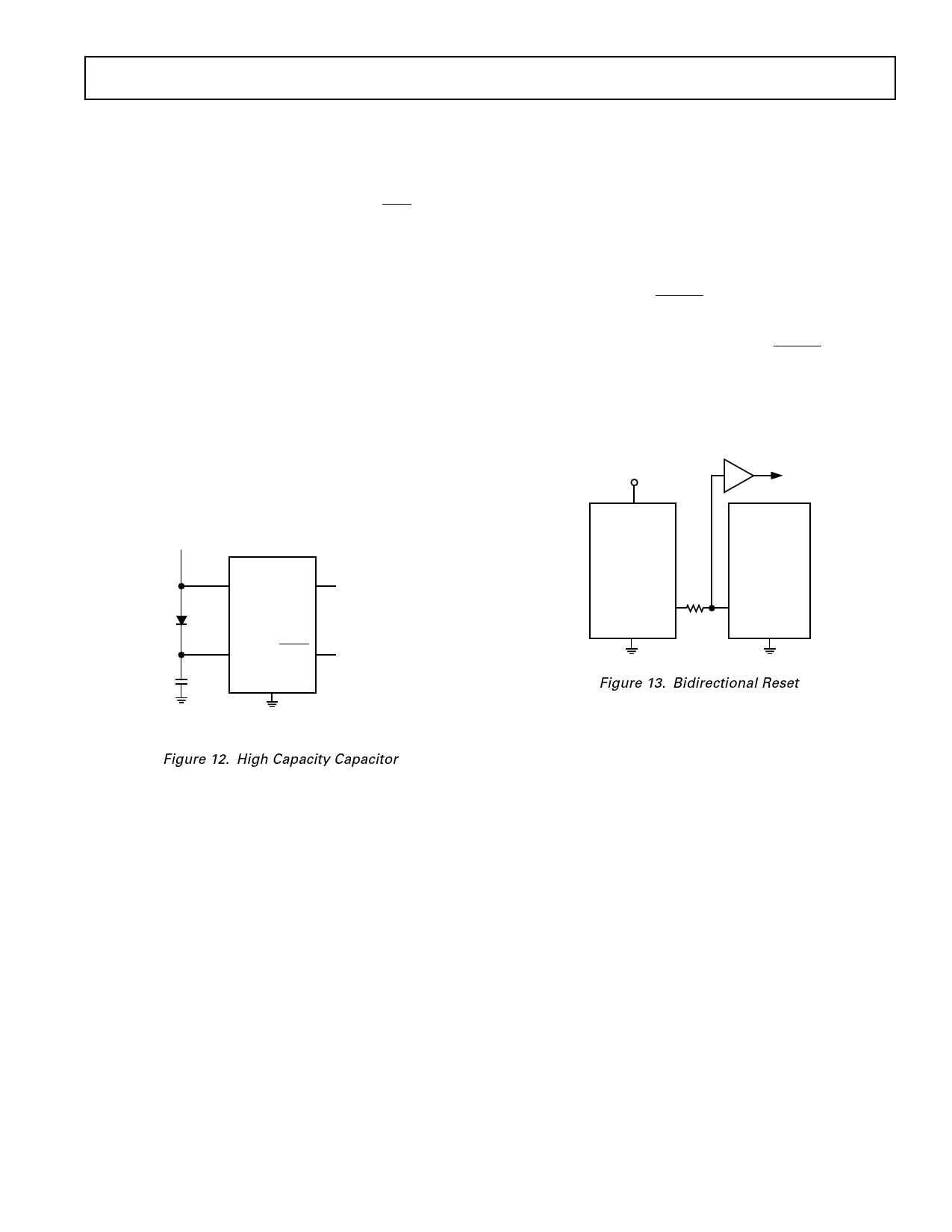
High Capacity Backup Capacitors
High capacity (0.1 µF or greater) capacitors may be used as a
backup power source. A typical application is shown in Fig-
ure 12.
+5V
VCC
VOUT
TO STATIC RAM
+
0.1F
VBATT
RESET
RESET*
GND
TO µP
Operation Without a Backup Supply
If a backup power source is not used, VBATT should be con-
nected to GND and VOUT should be connected to VCC.
Replacing the Backup Battery
The backup battery may be replaced without any danger of
spurious resetting when VCC is present. Since VCC is above the
reset threshold, a reset will not occur even if VBATT is floating
while a replacement battery is being inserted. This differs from
older generation products where leakage currents flowing out
VBATT could cause spurious resetting during battery replacement.
Ps With Bidirectional RESET
In order to prevent contention for microprocessors with a
bidirectional reset line, a current limiting resistor should be
inserted between the ADM69xA/ADM80xx RESET output pin
and the µP reset pin. This will limit the current to a safe level if
there are conflicting output reset levels. A suitable resistor value
is 4.7 kΩ. If the reset output is required for other uses, then it
should be buffered as shown in Figure 13.
BUFFERED
RESET
+5V
VCC
ADM690A
ADM692A
ADM802L
ADM802M
µP
RESET
GND
RESET
GND
Figure 13. Bidirectional Reset
*FOR ADM805L/ADM805M ONLY
Figure 12. High Capacity Capacitor
REV. 0
–7–
Share Link: 