VN16118L1 データシートの表示(PDF) - Vaishali Semiconductor
部品番号
コンポーネント説明
メーカー
VN16118L1 Datasheet PDF : 10 Pages
| |||
VN16118
Functional Block Description
Preliminary
Input Data Latch
The input data latch block latches the 10-bit TTL input parallel byte, TX<9:0>, on the rising
edge of the 125 MHz user-provided TX_CLK into the holding registers.
Parallel-to-Serial Converter
The received 10-bit TTL parallel input byte is converted to serial PECL level data stream by
the parallel-to-serial block, and is transmitted differentially to the line driver block at 1.25 Gbps.
The 8b/10b encoded data is transmitted sequentially with bit 0 being sent first.
Clock Generator
The 1250 MHz signal used for clocking the serial outputs is generated by the TX PLL block
based on the user-provided TX_CLK. This clock should have a ±100 ppm tolerance.
Internal Loopback
When EWRAP is set to a logic HIGH, the serial data stream generated by the transmitter is
looped back to the receiver path, instead of going out to the DOUT± pins. When in loopback
mode, a static logic 1 is transmitted at the line driver (DOUT+ is HIGH and DOUT- is LOW).
Signal Detect
Signal detect block is used to sense the serial input data stream at pins DIN±. If the serial input
is lower than 50 mV differentially, this block deasserts SIG_DET and sets the output, RX<9:0>,
to all logic ones. When the serial input at pins DIN± is greater than 50 mV, the signal is
directed to the receive path.
Equalizer and Slicer
The signal received from the line (DIN± pins) is distorted by the cable bandwidth. In order to
maintain a low bit-error rate, an equalizer is used to compensate for the signal loss. The slicer
recovers the differential low-level signal to a CMOS-level single-ended signal, for clock
recovery and data re-timing.
Clock Recovery
The serial input data stream contains both data and clock. The clock recovery block is used to
extract both data and clocks from this input. In addition to data, two clocks of 62.5 MHz are
recovered.
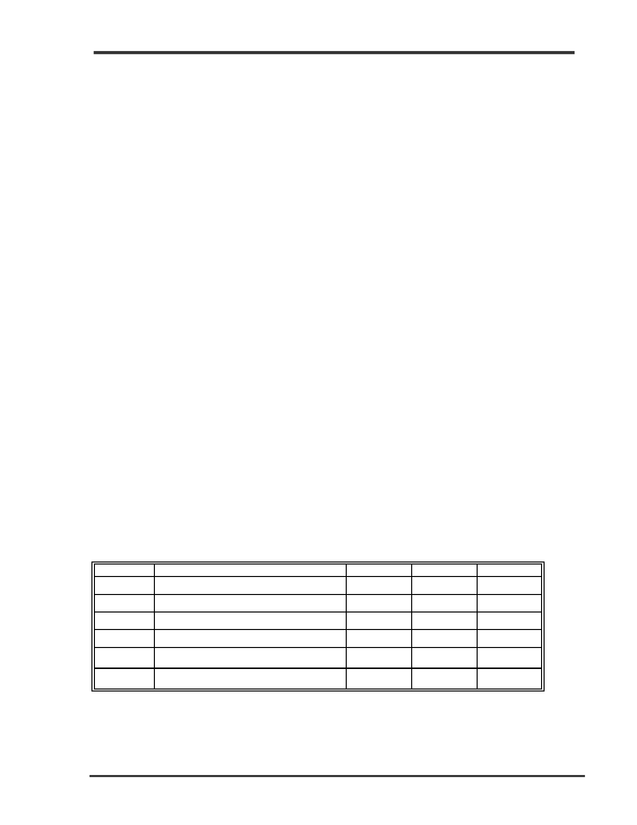
Table 2. Absolute Maximum Ratings
Symbol
Vcc
VIN,TTL
VIN,HS_IN
I O,TTL
Tstg
Parameter
Supply voltage
TTL Input Voltage
HS_IN Input Voltage
TTL Output Source Current
Storage Temperature
Tj
Junction Operating Temperature
Min.
-0.5
-0.7
2.0
-65
0
Max.
5.0
Vcc + 2.8
Vcc
13
+150
+150
Units
V
V
V
mA
°C
°C
Stresses above those listed under Absolute Maximum Ratings may cause permanent damage to the device.
These ratings are stress specifications only and correct functional operation of the device at these or any
other conditions above those listed in the operational sections of the specifications is not implied. Exposure
to absolute maximum rating conditions for extended periods may affect product reliability.
1999-12-15
Page 6
MDSN-0001-00
Vaishali Semiconductor l 747 Camden Avenue l Campbell l CA 95008 l Ph. 408.379.2900 l Fax 408.379.2937
Share Link: 