M59DR032 データシートの表示(PDF) - STMicroelectronics
部品番号
コンポーネント説明
メーカー
M59DR032 Datasheet PDF : 40 Pages
| |||
M59DR032A, M59DR032B
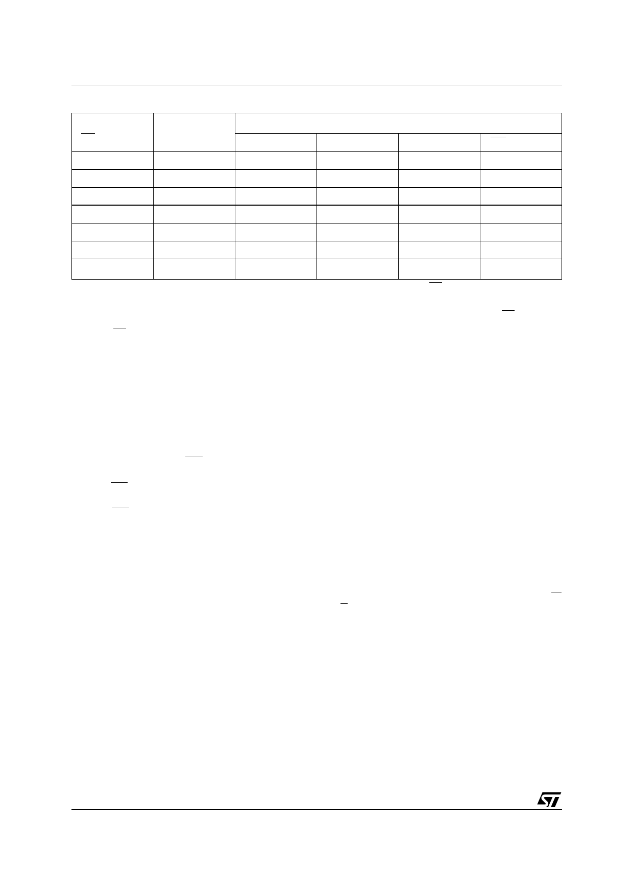
Table 13. Protection States (1)
Current State (2) Program/Erase
(WP, DQ1, DQ0)
Allowed
Protect
Next State After Event (3)
Unprotect
Lock
WP transition
100
yes
101
100
111
000
101
no
101
100
111
001
110
yes
111
110
111
011
111
no
111
110
111
011
000
yes
001
000
011
100
001
no
001
000
011
101
011
no
011
011
011
111 or 110 (4)
Note: 1. All blocks are protected at power-up, so the default configuration is 001 or 101 according to WP status.
2. Current state and Next state gives the protection status of a block. The protection status is defined by the write protect pin and by
DQ1 (= 1 for a locked block) and DQ0 (= 1 for a protected block) as read in the Autoselect instruction with A1 = VIH and A0 = VIL.
3. Next state is the protection status of a block after a Protect or Unprotect or Lock command has been issued or after WP has changed
its logic value.
4. A WP transition to VIH on a locked block will restore the previous DQ0 value, giving a 111 or 110.
Block Protect (BP), Block Unprotect (BU),
Block Lock (BL) Instructions. All blocks are
protected at power-up. Each block of the array has
two levels of protection against program or erase
operation. The first level is set by the Block Protect
instruction; a protected block cannot be pro-
grammed or erased until a Block Unprotect in-
struction is given for that block. A second level of
protection is set by the Block Lock instruction, and
requires the use of the WP pin, according to the
following scheme:
– when WP is at VIH, the Lock status is overridden
and all blocks can be protected or unprotected;
– when WP is at VIL, Lock status is enabled; the
locked blocks are protected, regardless of their
previous protect state, and protection status
cannot be changed. Blocks that are not locked
can still change their protection status, and pro-
gram or erase accordingly;
– the lock status is cleared for all blocks at power
up; once a block has been locked state can be
cleared only with a reset command. The protec-
tion and lock status can be monitored for each
block using the Autoselect (AS) instruction. Pro-
tected blocks will output a ‘1’ on DQ0 and locked
blocks will output a ‘1’ on DQ1.
Refer to Table 13 for a list of the protection states.
Block Erase (BE) Instruction. This instruction
uses a minimum of six write cycles. The Erase
Set-up command 80h is written to address 555h
on third cycle after the two Coded cycles. The
Block Erase Confirm command 30h is similarly
written on the sixth cycle after another two Coded
cycles and an address within the block to be
erased is given and latched into the memory.
Additional block Erase Confirm commands and
block addresses can be written subsequently to
erase other blocks in parallel, without further Cod-
ed cycles. All blocks must belong to the same
bank of memory; if a new block belonging to the
other bank is given, the operation is aborted. The
erase will start after an erase timeout period of
100µs. Thus, additional Erase Confirm commands
for other blocks must be given within this delay.
The input of a new Erase Confirm command will
restart the timeout period. The status of the inter-
nal timer can be monitored through the level of
DQ3, if DQ3 is '0' the Block Erase Command has
been given and the timeout is running, if DQ3 is '1',
the timeout has expired and the P/E.C. is erasing
the Block(s). If the second command given is not
an erase confirm or if the Coded cycles are wrong,
the instruction aborts, and the device is reset to
Read Array. It is not necessary to program the
block with 00h as the P/E.C. will do this automati-
cally before erasing to FFh. Read operations with-
in the same bank, after the sixth rising edge of W
or E, output the status register bits.
During the execution of the erase by the P/E.C.,
the memory accepts only the Erase Suspend ES
instruction; the Read/Reset RD instruction is ac-
cepted during the 100µs time-out period. Data
Polling bit DQ7 returns '0' while the erasure is in
progress and '1' when it has completed. The Tog-
gle bit DQ6 toggles during the erase operation,
and stops when erase is completed.
After completion the Status Register bit DQ5 re-
turns '1' if there has been an erase failure. In such
a situation, the Toggle bit DQ2 can be used to de-
termine which block is not correctly erased. In the
case of erase failure, a Read/Reset RD instruction
is necessary in order to reset the P/E.C.
10/39
Share Link: 