M59DR032 データシートの表示(PDF) - STMicroelectronics
部品番号
コンポーネント説明
メーカー
M59DR032 Datasheet PDF : 40 Pages
| |||
M59DR032A, M59DR032B
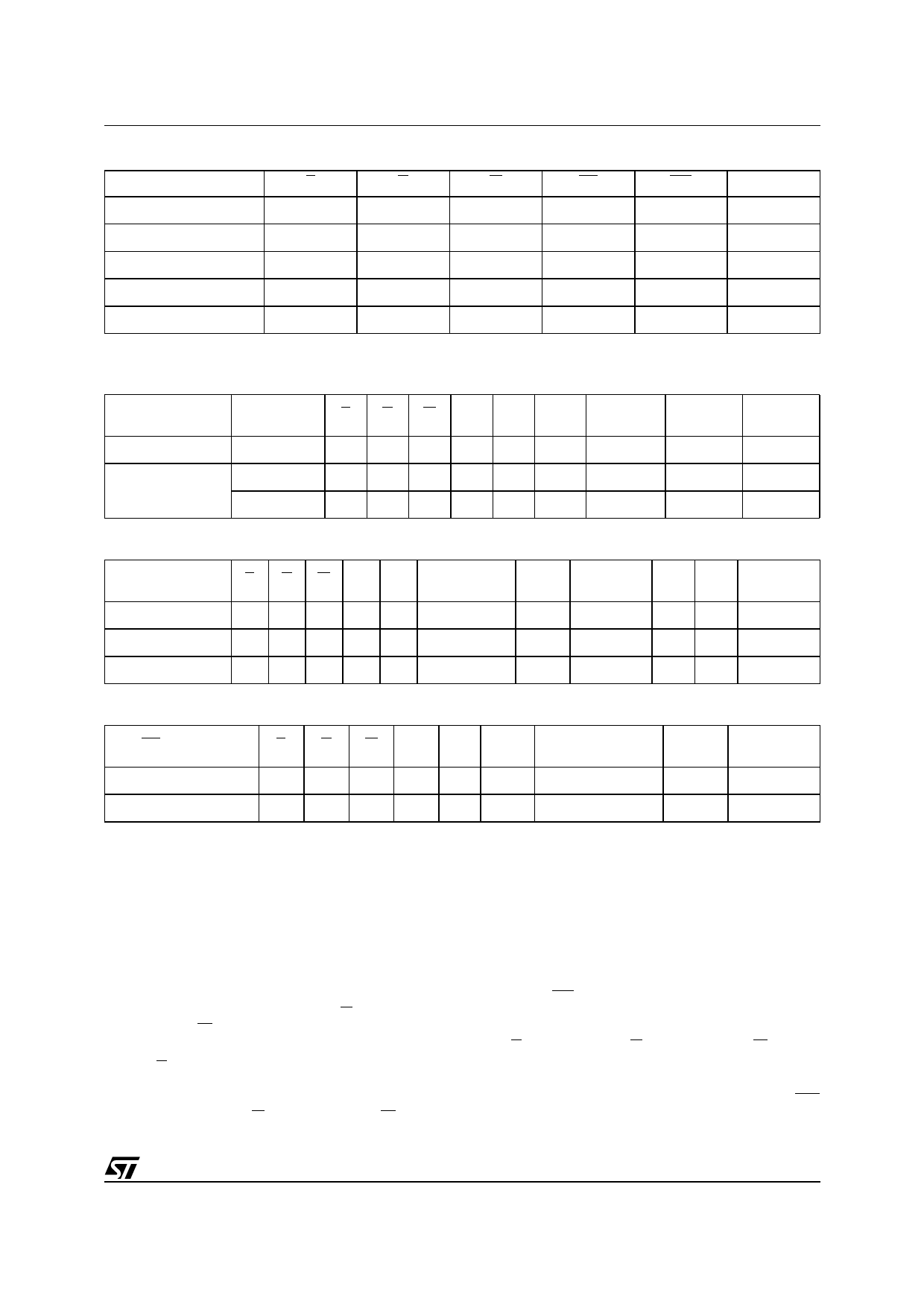
Table 8. User Bus Operations (1)
Operation
E
G
W
RP
WP
DQ15-DQ0
Write
VIL
VIH
VIL
VIH
VIH
Data Input
Output Disable
VIL
VIH
VIH
VIH
VIH
Hi-Z
Standby
VIH
X
X
VIH
VIH
Hi-Z
Reset / Power Down
X
X
X
VIL
VIH
Hi-Z
Block Locking
VIL
X
X
VIH
VIL
X
Note: 1. X = Don’t care.
Table 9. Read Electronic Signature (AS and Read CFI instructions)
Code
Device
E
G
W
A0
A1
A7-A2
Other
Addresses
DQ15-DQ8
DQ7-DQ0
Manufacturer Code
VIL VIL VIH VIL VIL
0 Don’t Care
00h
20h
M59DR032A VIL VIL VIH VIH VIL
0 Don’t Care
00h
A0h
Device Code
M59DR032B VIL VIL VIH VIH VIL
0 Don’t Care
00h
A1h
Table 10. Read Block Protection (AS and Read CFI instructions)
Block Status
E G W A0 A1
A20-A12
A7-A2
Other
Addresses
DQ0
DQ1
DQ15-DQ2
Protected Block
VIL VIL VIH VIL VIH Block Address 0
Don’t Care 1
0
0000h
Unprotected Block VIL VIL VIH VIL VIH Block Address 0
Don’t Care 0
0
0000h
Locked Block
VIL VIL VIH VIL VIH Block Address 0
Don’t Care X
1
0000h
Table 11. Read Configuration Register (AS and Read CFI instructions)
RP Function
E
G
W A0 A1 A7-A2 Other Addresses
Reset
Reset/Power Down
VIL VIL VIH VIH VIH
0
VIL VIL VIH VIH VIH
0
Don’t Care
Don’t Care
DQ10
0
1
DQ9-DQ0
DQ15-DQ11
Don’t Care
Don’t Care
Dual Bank Operations. The Dual Bank allows to
read data from one bank of memory while a pro-
gram or erase operation is in progress in the other
bank of the memory. Read and Write cycles can
be initiated for simultaneous operations in different
banks without any delay. Status Register during
Program or Erase must be monitored using an ad-
dress within the bank being modified.
Output Disable. The data outputs are high im-
pedance when the Output Enable G is at VIH with
Write Enable W at VIH.
Standby. The memory is in standby when Chip
Enable E is at VIH and the P/E.C. is idle. The pow-
er consumption is reduced to the standby level
and the outputs are high impedance, independent
of the Output Enable G or Write Enable W inputs.
Automatic Standby. When in Read mode, after
150ns of bus inactivity and when CMOS levels are
driving the addresses, the chip automatically en-
ters a pseudo-standby mode where consumption
is reduced to the CMOS standby value, while out-
puts still drive the bus.
Power Down. The memory is in Power Down
when the Configuration Register is set for Power
Down and RP is at VIL. The power consumption is
reduced to the Power Down level, and Outputs are
in high impedance, independent of the Chip En-
able E, Output Enable G or Write Enable W inputs.
Block Locking. Any combination of blocks can
be temporarily protected against Program or
Erase by setting the lock register and pulling WP
to VIL (see Block Lock instruction).
7/39
Share Link: 