UPC4081C データシートの表示(PDF) - NEC => Renesas Technology
部品番号
コンポーネント説明
メーカー
UPC4081C Datasheet PDF : 12 Pages
| |||
µPC4081
ABSOLUTE MAXIMUM RATINGS (TA = 25°C)
Parameter
Symbol
Ratings
Unit
Voltage between V+ and V– Note 1
V+ – V–
–0.3 to +36
V
Differential Input Voltage
VID
Input VoltageNote 2
VI
Output VoltageNote 3
VO
Power Dissipation
C PackageNote 4
PT
G2 PackageNote 5
Output Short Circuit DurationNote 6
±30
V
V––0.3 to V+ +0.3
V
V––0.3 to V+ +0.3
V
350
mW
440
mW
Indefinite
sec
Operating Ambient Temperature
TA
–20 to +80
°C
Storage Temperature
Tstg
–55 to +125
°C
Notes 1. Reverse connection of supply voltage can cause destruction.
2. The input voltage should be allowed to input without damage or destruction. Even during the transition period
of supply voltage, power on/off etc., this specification should be kept. The normal operation will establish when
the both inputs are within the Common Mode Input Voltage Range of electrical characteristics.
3. This specification is the voltage which should be allowed to supply to the output terminal from external without
damage or destructive. Even during the transition period of supply voltage, power on/off etc., this specification
should be kept. The output voltage of normal operation will be the Output Voltage Swing of electrical
characteristics.
4. Thermal derating factor is –5.0 mV/°C when operating ambient temperature is higher than 55°C.
5. Thermal derating factor is –4.4 mV/°C when operating ambient temperature is higher than 25°C.
6. Pay careful attention to the total power dissipation not to exceed the absolute maximum ratings, Note 4 and
Note 5.
RECOMMENDED OPERATING CONDITIONS
Parameter
Supply Voltage
5 Output Current
5 Capacitive Load (AV = +1, Rf = 0 Ω)
Symbol
MIN.
TYP.
MAX.
Unit
V±
±5
±16
V
IO
±10
mA
CL
100
pF
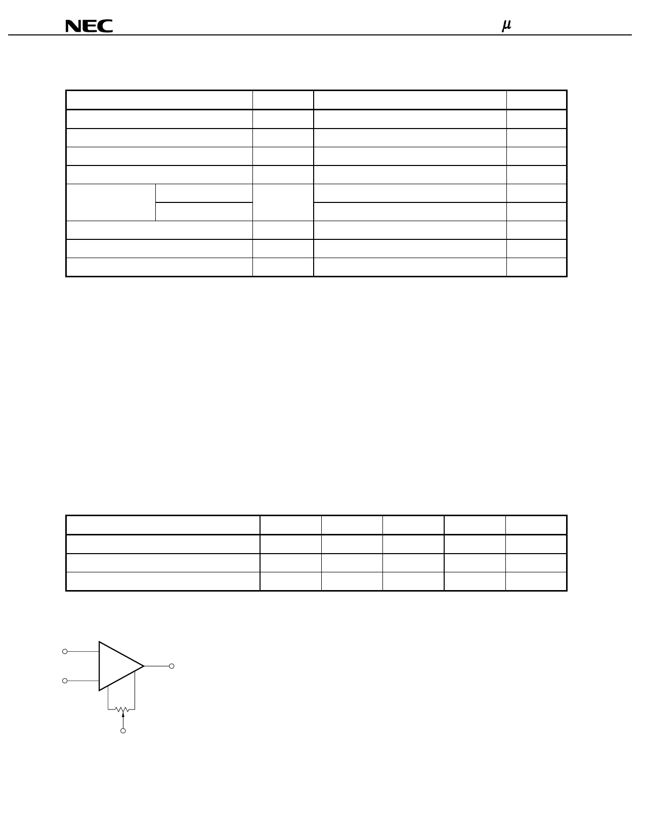
OFFSET VOLTAGE NULL CIRCUIT
2_
6
5
+
3
1
100 kΩ
VR1
_
V
2
5 Remark The OFFSET NULL pins should be left
open or connected to V– via a resistor as
shown in the left figure. Don't connect to
any lines other than V–, otherwise
mulfunction, degradation, or failure may
occur.
Data Sheet G15343EJ3V0DS
Share Link: 