UPC4081C データシートの表示(PDF) - NEC => Renesas Technology
部品番号
コンポーネント説明
メーカー
UPC4081C Datasheet PDF : 12 Pages
| |||
µPC4081
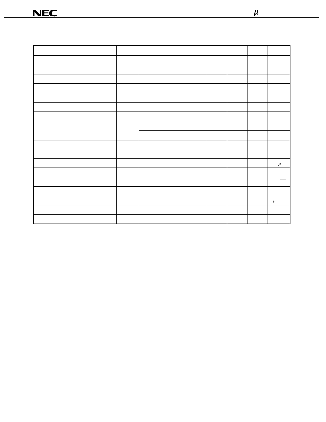
ELECTRICAL CHARACTERISTICS (TA = 25°C, V± = ±15 V)
Parameter
Input Offset Voltage
Input Offset Current Note 7
Input Bias Current Note 7
Large Signal Voltage Gain
Supply Current
Common Mode Rejection Ratio
Supply Voltage Rejection Ratio
Output Voltage Swing
Common Model Input Voltage Range
Symbol
Conditions
VIO
RS ≤ 50 Ω
IIO
IB
AV
RL ≥ 2 kΩ , VO = ±10 V
ICC
IO = 0 A
CMR
SVR
Vom
RL ≥ 10 kΩ
RL ≥ 2 kΩ
VICM
Slew Rate
Unity Gain Frequency
Input Equivalent Noise Voltage Density
Input Offset Voltage
Average VIO Temperature Drift
Input Offset CurrentNote 7
Input Bias CurrentNote 7
SR
funity
en
VIO
∆VIO/∆T
IIO
IB
AV = 1
RS = 100 Ω, f = 1 kHz
RS ≤ 50 Ω, TA = –20 to +70°C
TA = –20 to +70°C
TA = –20 to +70°C
TA = –20 to +70°C
MIN.
25000
70
70
±12
±10
±10
TYP.
±5
±5
30
200000
2.0
76
76
±13.5
±12
+15
–12.7
13
3
25
±10
MAX.
±15
±200
400
2.8
±20
±5
10
Unit
mV
pA
pA
mA
dB
dB
V
V
V
V/µs
MHz
nV/√Hz
mV
µV/°C
nA
nA
Notes 7. Input bias currents flow into IC. Because each currents are gate leak current of P-channel J-FET on input
stage. And that are temperature sensitive. Short time measuring method is recommendable to maintain the
junction temperature close to the operating ambient temperature.
Data Sheet G15343EJ3V0DS
3
Share Link: 