UC2844BD(2008) データシートの表示(PDF) - ON Semiconductor
部品番号
コンポーネント説明
メーカー
UC2844BD Datasheet PDF : 19 Pages
| |||
UC3844B, UC3845B, UC2844B, UC2845B
ELECTRICAL CHARACTERISTICS (VCC = 15 V [Note 11], RT = 10 k, CT = 3.3 nF. For typical values TA = 25°C, for min/max
values TA is the operating ambient temperature range that applies [Note 12], unless otherwise noted.)
UC284XB
UC384XB, XBV
Characteristic
Symbol
Min Typ Max Min Typ Max Unit
PWM SECTION
Duty Cycle
Maximum (UC284XB, UC384XB)
Maximum (UC384XBV)
Minimum
TOTAL DEVICE
Power Supply Current
Startup (VCC = 6.5 V for UCX845B,
Startup (VCC = 14 V for UCX844B, BV)
Operating (Note 11)
DC(max)
DC(min)
ICC
%
47
48
50
47
48
50
−
−
−
46
48
50
−
−
0
−
−
0
mA
−
0.3 0.5
−
0.3 0.5
−
12
17
−
12
17
Power Supply Zener Voltage (ICC = 25 mA)
VZ
30
36
−
30
36
−
V
11. Adjust VCC above the Startup threshold before setting to 15 V.
12. Low duty cycle pulse techniques are used during test to maintain junction temperature as close to ambient as possible.
Tlow = 0°C for UC3844B, UC3845B
= − 25°C for UC2844B, UC2845B
Thigh = + 70°C for UC3844B, UC3845B
= + 85°C for UC2844B, UC2845B
= − 40°C for UC3844BV, UC3845BV
= +105°C for UC3844BV, UC3845BV
80
50
20
8.0
VCC = 15 V
TA = 25°C
75
ÄÄÄÄÄ 1. CT = 10 nF
2. CT = 5.0 nF
ÄÄÄÄÄ 70 3. CT = 2.0 nF
4. CT = 1.0 nF
ÄÄÄÄÄ 5. CT = 500 pF
65 6. CT = 200 pF
ÄÄÄÄÄÄÄÄÄÄ 7. CT = 100 pF
3
24
1
5.0
60
7
2.0
NOTE: Output switches at
1/2 the oscillator frequency
0.8
10 k 20 k
50 k
100 k
200 k
500 k
fOSC, OSCILLATOR FREQUENCY (kHz)
For
RT
u
5
Kf
X
1.72
RTCT
1.0 M
55
50
10 k
5
6
20 k
50 k 100 k 200 k
500 k 1.0 M
fOSC, OSCILLATOR FREQUENCY (kHz)
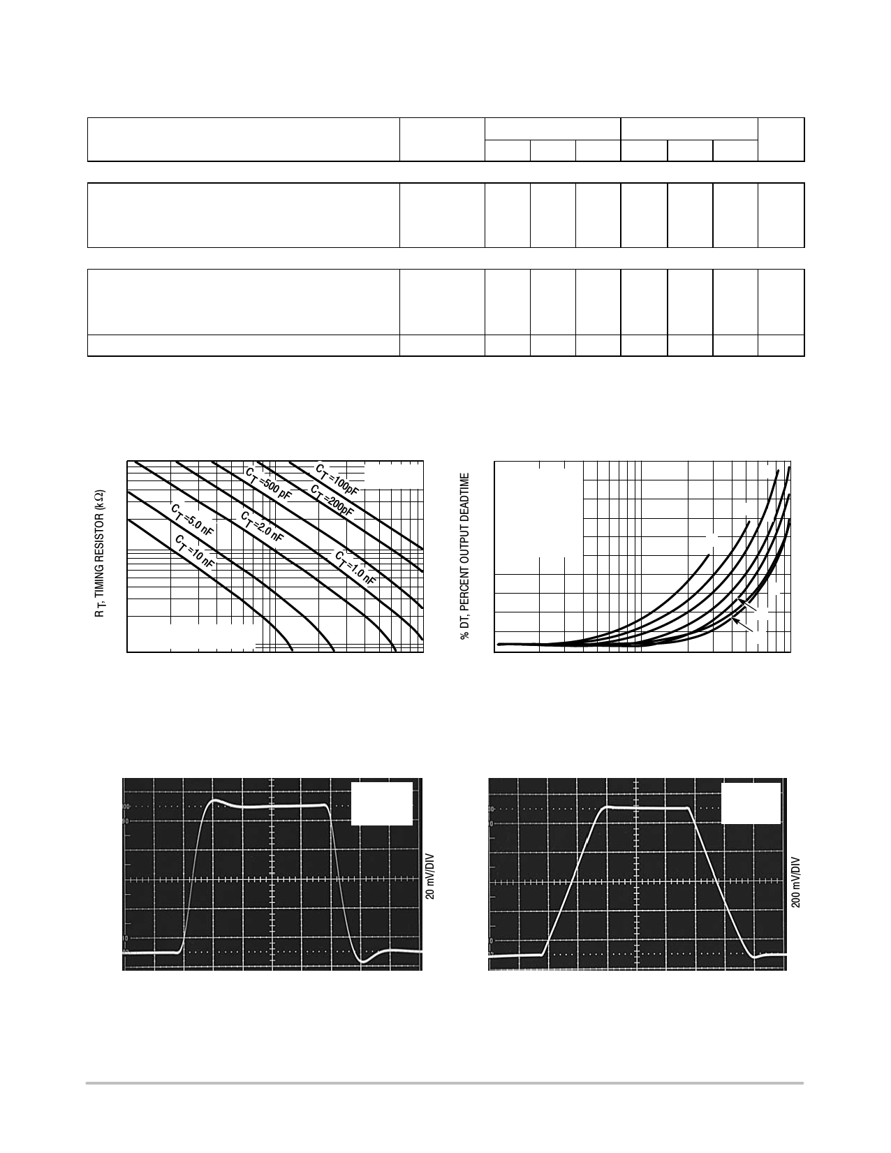
Figure 2. Timing Resistor
versus Oscillator Frequency
Figure 3. Output Deadtime
versus Oscillator Frequency
2.55 V
VCC = 15 V
AV = -1.0
TA = 25°C
3.0 V
VCC = 15 V
AV = -1.0
TA = 25°C
2.5 V
2.5 V
2.45 V
0.5 ms/DIV
Figure 4. Error Amp Small Signal
Transient Response
2.0 V
1.0 ms/DIV
Figure 5. Error Amp Large Signal
Transient Response
http://onsemi.com
4
Share Link: 